
power supply circuit
Index 7
Full bridge inverter circuit full bridge inverter circuit diagram
Published:2014/2/18 21:52:00 Author: | Keyword: Full bridge inverter circuit full bridge inverter circuit diagram,
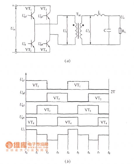
Single-phase inverter circuit is push-pull type, half bridge type and bridge type, among them, the full bridge inverter circuit for use in the most common. Single phase full bridge inverter circuit principle as shown in figure (a). (b) excitation signal and the output voltage waveform. (View)
View full Circuit Diagram | Comments | Reading(1682)
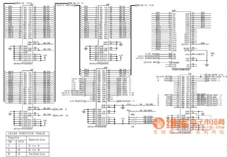
ICETEK C6711 -- A principle figure 11
Published:2014/2/18 21:49:00 Author: | Keyword: ICETEK C6711 -- A principle figure 11,
ICETEK - C6711 - A principle as shown in figure 11 (View)
View full Circuit Diagram | Comments | Reading(1010)
Deformation of the half bridge converter principle of electric circuit diagram
Published:2014/2/18 21:46:00 Author: | Keyword: Deformation of the half bridge converter principle of electric circuit diagram,
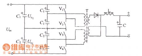
For high input, high power output, generally USES the way of circuit as shown. In the circuit, switching devices V1, V2, V3 and V4 as a group, both in series and can reduce the single pipe pressure values. In the practical application circuit switch device in the V1, V2, V3 and V4 can adopt double pipe or in parallel, can solve the problem of large current output. Common transformer can improve the utilization efficiency of transformer, and has the ability to resist imbalance. In series of half bridge circuit, power transformation V1, V2 and V3, V4 each maximum withstand voltage value of the switch tube is only ucs 1 or Uc2 value, if C1 = C2, the ucs 1 = Uc2 = Uin / 2 value, therefore can choose to reduce the pressure switch tube. Another V1, V2, V3 and V4 manifold can be used in parallel work, increasing the capacity of the output current; T can work on the positive and negative direction for transformer, greatly improve the efficiency of the transformer. In view of the above advantages, the circuit has been more widely used, especially in the occasion of high input voltage and high power output, its application is becoming more common. (View)
View full Circuit Diagram | Comments | Reading(913)
Double is excitation converter principle of electric circuit diagram
Published:2014/2/18 21:38:00 Author: | Keyword: Double is excitation converter principle of electric circuit diagram,
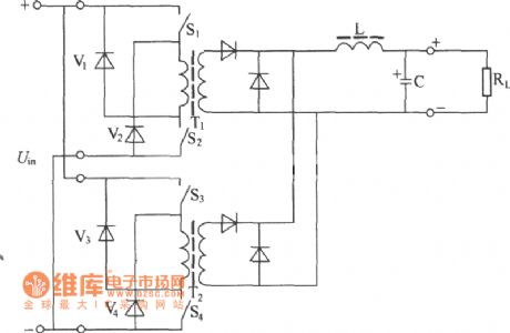
When need larger output power, generally adopt the double normal shock type conversion circuit of voltage overlay, as shown. Circuit features: (1) two normal shock type conversion circuit in parallel, T1 and T2 inverting 180 o drive, a doubling of the power and output frequency doubled, ripple and dynamic response is improved; (2) the series S1, S2, S3, S4 series), switch tube pressure by half; (3) to cancel the feedback coil, V1, V2, VpV4 are can feed path, reduce the production technology of transformer and other requirements; (4) with dead zone limit, features two parts there is no common mode circuit conduction problem, and high reliability. Characteristic: normal shock: conduction type feeder to load, when the time L power supply to the load. Pressure: single pipe is excited, maximum voltage switch tube is 2 uin. Two pipe is shock: switch tube maximum voltage for Uin. : transformer utilization rate is not high (only using the first quadrant hysteresis loop), the production process to add on the feed can coil. Purpose: because the two pipe is shock parallel circuit has big output power, output pulse frequency doubling, easy to filter, switch tube pressure by half (about the input voltage Ui. , so widely used in high power conversion circuit, is considered to be high reliability at present, manufacturing is not the main circuit of a complex. (View)
View full Circuit Diagram | Comments | Reading(909)
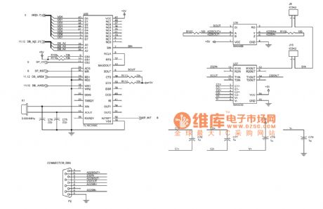
ICETEK C6711 -- A principle figure 12
Published:2014/2/18 21:36:00 Author: | Keyword: ICETEK C6711 -- A principle figure 12,
ICETEK - C6711 - A principle as shown in figure 12 (View)
View full Circuit Diagram | Comments | Reading(769)
The basic composing of switch rectifier circuit diagram
Published:2014/2/18 21:34:00 Author: | Keyword: The basic composing of switch rectifier circuit diagram,

Switch rectifier is mainly composed of four parts: input circuit, power transformer, rectifier, filter circuit and control circuit, as shown. Input circuit will ac input voltage rectifier filter into a relatively flat high-voltage dc voltage, the power converter converts it to the high frequency pulse voltage, then through rectifying filter circuit converts the high frequency pulse voltage steady dc voltage, output to the load. Control circuit of the role is to ensure the stability of the output dc voltage and is adjustable. (View)
View full Circuit Diagram | Comments | Reading(1024)
ICETEK C6711 -- A principle in figure 13
Published:2014/2/17 23:34:00 Author: | Keyword: ICETEK C6711 -- A principle in figure 13,
ICETEK - C6711 - A principle as shown in figure 13 (View)
View full Circuit Diagram | Comments | Reading(762)
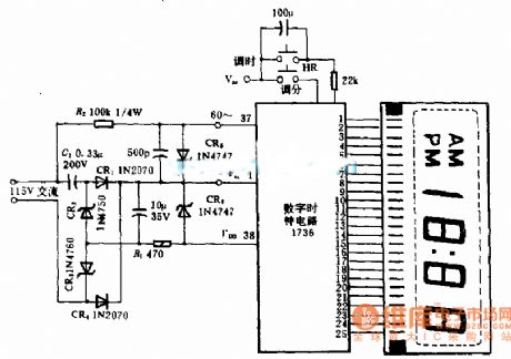
10000 b timing circuit diagram (seconds, minutes)
Published:2014/2/17 23:30:00 Author: | Keyword: 10000 b timing circuit diagram (seconds, minutes),

10000 b timing circuit diagram (seconds, minutes)
(View)
View full Circuit Diagram | Comments | Reading(1083)
High resistance distribution circuit diagram
Published:2014/2/17 23:29:00 Author: | Keyword: High resistance distribution circuit diagram,
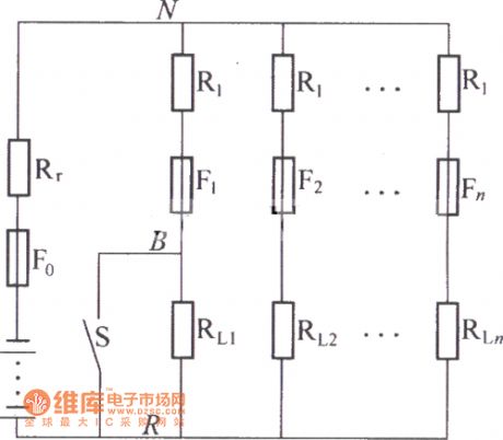
As shown in figure for high resistance distribution circuit diagram. It with low resistance distribution in the load distribution is the significant difference between concatenated certain resistance current limiting resistor R1, general value for 5 times ~ l0 times of battery internal resistance. If a shunt short-circuit happened at this moment, the system voltage drop and recoil peak voltage is small, this is because the R1 limiting the short-circuit current, at the same time L x di/dt is lesser also. As shown is voltage variation between N and R. Selecting suitable R1 and Rr, can make the voltage change between N and R within the scope of the power system permitted error, the system of independent among load, mutually influence. Over the road purpose to enhance the reliability of communication system. In practice, can be developed the application of multilevel high resistance distribution. (View)
View full Circuit Diagram | Comments | Reading(936)
12 or 24 h clock circuit diagram
Published:2014/2/17 23:15:00 Author: | Keyword: 12 or 24 h clock circuit diagram,
12 or 24 h clock circuit diagram
(View)
View full Circuit Diagram | Comments | Reading(1207)
ICETEK C6711 -- A principle figure 14
Published:2014/2/17 23:13:00 Author: | Keyword: ICETEK C6711 -- A principle figure 14,
ICETEK - C6711 - A principle as shown in figure 14 (View)
View full Circuit Diagram | Comments | Reading(707)
ICETEK C6711 -- A principle figure 15
Published:2014/2/17 23:09:00 Author: | Keyword: ICETEK C6711 -- A principle figure 15,

ICETEK - C6711 - A principle as shown in figure 15 (View)
View full Circuit Diagram | Comments | Reading(719)
Station power supply distribution system diagram
Published:2014/2/17 23:04:00 Author: | Keyword: Station power supply distribution system diagram,
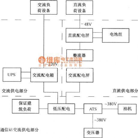
Communication power supply points for communications equipment. Direct supply power communication power supply is a key part, the body of the power station and power station also includes interrupt the guarantee of building load allows for short periods of time, such as computer room air conditioning, etc. General station of power supply as shown. (View)
View full Circuit Diagram | Comments | Reading(819)
ICETEK C6711 -- A principle figure 16
Published:2014/2/17 21:37:00 Author: | Keyword: ICETEK C6711 -- A principle figure 16,
ICETEK - C6711 - A principle as shown in figure 16 (View)
View full Circuit Diagram | Comments | Reading(787)
Dongfeng Peugeot Citroen Picasso 2.0L sedan headlight regulator circuit
Published:2014/2/17 21:03:00 Author:lynne | Keyword: Dongfeng Peugeot Citroen Picasso 2.0L sedan headlight regulator circuit,
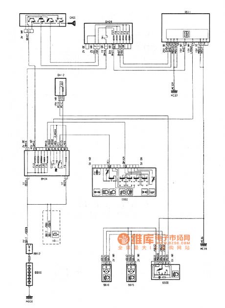
Dongfeng Peugeot Citroen Picasso 2.0L sedan headlight regulator circuit shown in Figure:
(View)
View full Circuit Diagram | Comments | Reading(746)
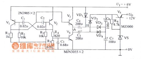
Dc voltage double power supply circuit diagram
Published:2014/2/16 21:32:00 Author: | Keyword: Dc voltage double power supply circuit diagram,
View full Circuit Diagram | Comments | Reading(1192)
LG510 type mobile phone line circuit principle diagram
Published:2014/2/7 20:01:00 Author: | Keyword: LG510 type mobile phone line circuit principle diagram,
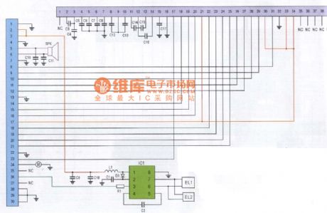
As shown in figure LG510 type mobile phone line circuit principle diagram (View)
View full Circuit Diagram | Comments | Reading(849)
60 h timer circuit diagram
Published:2014/2/7 19:54:00 Author: | Keyword: 60 h timer circuit diagram,
60 h timer circuit diagram
(View)
View full Circuit Diagram | Comments | Reading(982)
Car clock circuit diagram
Published:2014/2/7 19:54:00 Author: | Keyword: Car clock circuit diagram,
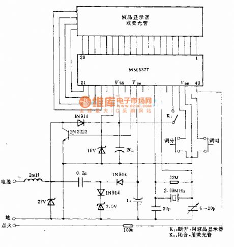
Car clock circuit diagram
(View)
View full Circuit Diagram | Comments | Reading(1409)
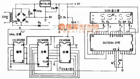
LCD watch circuit diagram
Published:2014/2/7 19:52:00 Author: | Keyword: LCD watch circuit diagram,
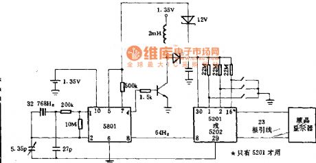
LCD watch circuit diagram
(View)
View full Circuit Diagram | Comments | Reading(1075)
| Pages:7/291 1234567891011121314151617181920Under 20 |
Circuit Categories
power supply circuit
Amplifier Circuit
Basic Circuit
LED and Light Circuit
Sensor Circuit
Signal Processing
Electrical Equipment Circuit
Control Circuit
Remote Control Circuit
A/D-D/A Converter Circuit
Audio Circuit
Measuring and Test Circuit
Communication Circuit
Computer-Related Circuit
555 Circuit
Automotive Circuit
Repairing Circuit