
power supply circuit
Index 2
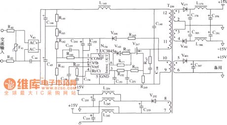
3844 switching power supply circuit
Published:2014/3/17 20:59:00 Author:lynne | Keyword: 3844 switching power supply circuit,
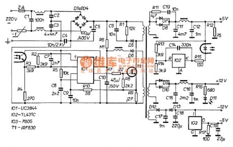
3844 switching power supply circuit shown as follow: (View)
View full Circuit Diagram | Comments | Reading(4811)
ZTE mobile phone charger circuit diagram
Published:2014/3/16 21:12:00 Author:lynne | Keyword: ZTE mobile phone charger circuit diagram,
ZTE mobile phone charger circuit diagram as shown:
(View)
View full Circuit Diagram | Comments | Reading(3704)
DC low-voltage regulated power supply circuit
Published:2014/3/16 21:11:00 Author:lynne | Keyword: DC low-voltage regulated power supply circuit, NE555
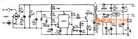
Switching power supply portion VD1-VD4, R1, C1, C2 smoothing circuit composed of the rectifier . NE555 and R2, R3, C4, VD6 other components multivibrator circuit , its frequency is about 20KHz. R4, C3, VD5 composition buck regulator circuit , as NE555 provides 12V power supply. High-power tube VT1 and transformer T constitutes a switching circuit . NE555 VT1 working state by the foot control of ③ , the conduction time is determined by the pulse width , the pulse width can be changed to adjust R3 . Wider pulse width , the output voltage increases ; narrowing the pulse width , the output voltage is reduced. VT2 and R8, R9, C6 composition overcurrent protection circuit . When overloaded or short-circuit fault , VT2 conduction, forced NE555 reset stop vibration , thereby protecting VT1 without damage. C7, R10 to protect the network and prevent the breakdown of VT1 ce knot instantaneous pulse . After two secondary windings are rectified and filtered output of 20V and 12V.In order to make simple , switching power supply designed to not automatically regulated , its function is similar to a transformer , only to realize the light of the antihypertensive effect of isolation , voltage regulation implemented by the back of the regulator circuit . 12V DC voltage by 7805 the +5 V output voltage ; 20V adjustable DC voltage to the voltage regulator circuit . No common ground between the two , in order to add or subtract a combination of a variety of output voltages.DC low voltage power supply circuit shown in Figure:
(View)
View full Circuit Diagram | Comments | Reading(3507)
7812 regulated power supply circuit
Published:2014/3/11 22:58:00 Author:lynne | Keyword: 7812 regulated power supply circuit, 7812
7812 regulated power supply circuit shown as follow:
(View)
View full Circuit Diagram | Comments | Reading(2202)
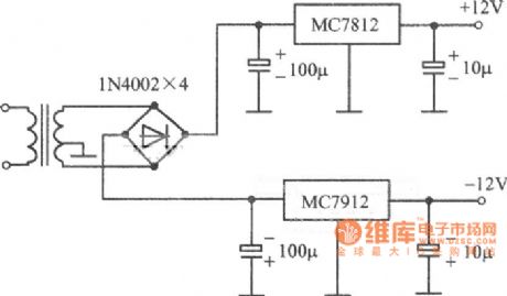
7815 regulated power supply circuit
Published:2014/3/11 22:49:00 Author:lynne | Keyword: 7815 regulated power supply circuit, 7815
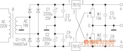
Continuously adjustable dual power ( positive and negative symmetrical power supply ) . This circuit consists of a symmetrical connection 7815 and a 7915 three-terminal regulator , you can get a set of positive and negative symmetrical power supply, and the output voltage can be adjusted individually each , can also be synchronized adjustment.Circuit as shown , the AC output from the transformer voltage by 18V double rectifier D1 ~ D4 , C1, C2 obtained by filtering a DC voltage, wherein the dual power transformer center tap as a common ground, and each of the positive and negative of the DC voltage access ① 7815 and 7915 feet of ③ feet. ③ 7815 feet of sliding contacts connected to the potentiometer W2 of d , the pin 7915 to the potentiometer ① sliding contact piece W1 C on . When the contacts C slide 0 when terminated , the regulator W2, to a and end get +6 ~ +15 V Forward variable voltage ; contacts If d slide 0 termination , the regulator W1, in the b side can get -6 ~-15V negative variable voltage, W1, W2 into coaxial potentiometer obtain the symmetrical adjustable power supply , the output voltage is continuously adjustable between ± 6V ~ ± 15V, can be synchronized adjustment purposes.7815,7915 heatsink should be installed on the three-terminal voltage regulator circuit block , do heat dissipation .7815 regulated power supply circuit shown in Fig.
(View)
View full Circuit Diagram | Comments | Reading(3400)
The DMA auxiliary power circuit diagram
Published:2014/3/9 22:50:00 Author: | Keyword: The DMA auxiliary power circuit diagram,
View full Circuit Diagram | Comments | Reading(1938)
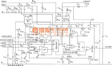
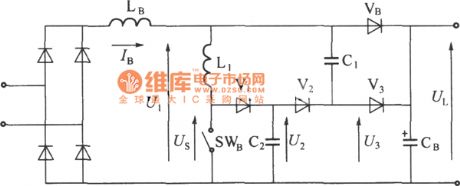
The DMA booster/power factor correction control circuit diagram
Published:2014/3/9 22:49:00 Author: | Keyword: The DMA booster/power factor correction control circuit diagram,
View full Circuit Diagram | Comments | Reading(1599)
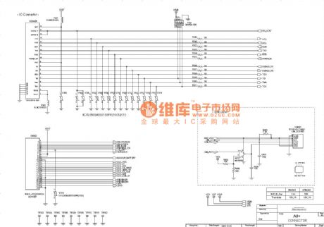
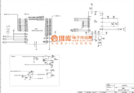
Amoi A8 + - LCD circuit principle diagram
Published:2014/3/9 22:46:00 Author: | Keyword: Amoi A8 + - LCD circuit principle diagram,
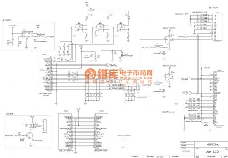
Amoi A8 + as shown - LCD circuit principle diagram (View)
View full Circuit Diagram | Comments | Reading(1773)
The DMA lossless absorption buffer circuit diagram
Published:2014/3/9 22:45:00 Author: | Keyword: The DMA lossless absorption buffer circuit diagram,
View full Circuit Diagram | Comments | Reading(1588)
Booster type power factor correction principle of electric circuit diagram
Published:2014/3/9 22:44:00 Author: | Keyword: Booster type power factor correction principle of electric circuit diagram,
View full Circuit Diagram | Comments | Reading(1479)
Amoi A8 + - IO mouth - SIM card schematic circuit diagram
Published:2014/3/9 22:41:00 Author: | Keyword: Amoi A8 + - IO mouth - SIM card schematic circuit diagram,
Amoi A8 + as shown - IO mouth - SIM card schematic circuit diagram (View)
View full Circuit Diagram | Comments | Reading(1751)
Mazda engine performance diagram (1.3 L)
Published:2014/3/9 22:38:00 Author: | Keyword: Mazda engine performance diagram (1.3 L),
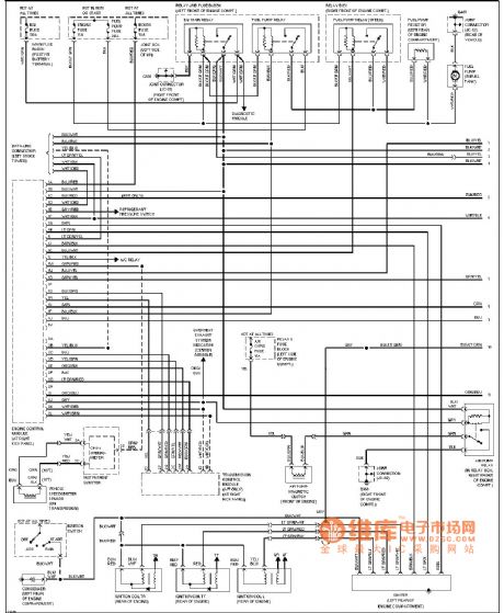
Mazda engine performance diagram as shown (1.3 L) (View)
View full Circuit Diagram | Comments | Reading(1759)
Amoi A8 + - 16 chord and logic circuit principle diagram
Published:2014/3/9 22:36:00 Author: | Keyword: Amoi A8 + - 16 chord and logic circuit principle diagram,
Amoi A8 + as shown - 16 chord and logic circuit principle diagram (View)
View full Circuit Diagram | Comments | Reading(1373)
DMAl2 input circuit diagram
Published:2014/3/9 22:34:00 Author: | Keyword: DMAl2 input circuit diagram,

View full Circuit Diagram | Comments | Reading(1357)
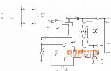
TEA1523P power circuit
Published:2014/3/9 21:39:00 Author:lynne | Keyword: TEA1523P power circuit, TEA1523P
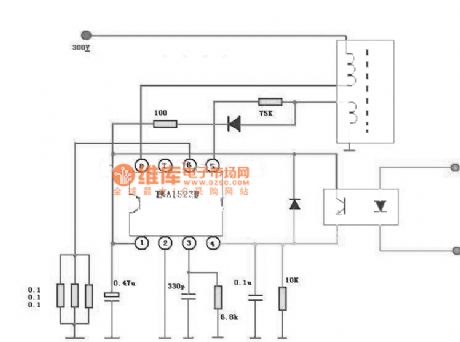
TEA1523P power circuit shown as follow:
(View)
View full Circuit Diagram | Comments | Reading(5855)
uc3842 switching power supply circuit
Published:2014/3/6 20:56:00 Author:lynne | Keyword: uc3842 switching power supply circuit, uc3842

uc3842 switching power supply circuit shown in figure:
(View)
View full Circuit Diagram | Comments | Reading(14215)
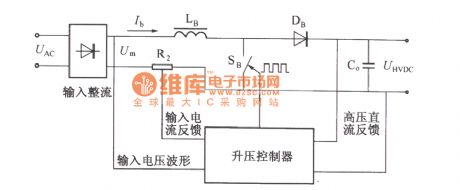
DMAl2 main circuit principle diagram
Published:2014/3/6 20:13:00 Author: | Keyword: DMAl2 main circuit principle diagram,
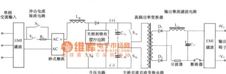
As shown for simplified DMA12 main circuit principle diagram. It is mainly composed of input circuit and electromagnetic interference (EMI) filter circuit, impact current limiting circuit, input rectifier filter circuit, booster/power factor correction circuit and absorption circuit, a half-bridge power conversion circuit, the output rectifier filter circuit, etc. Compared with DMA10, DMA12 adopted single phase input, booster/power factor correction method and the lossless absorption buffer circuit, and half bridge DC/DC power conversion and output rectifier filter part like the DMA10. (View)
View full Circuit Diagram | Comments | Reading(1388)
DMAl2 constitute a circuit diagram
Published:2014/3/6 20:13:00 Author: | Keyword: DMAl2 constitute a circuit diagram,
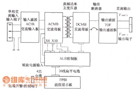
DMA12 intelligent switch rectifier module by the ac input board (ACIB), the exchange motherboard (ACMB), dc motherboard (DCMB), output filter plate (TOF), control panel (propagated), shown earlier (FPBI) six boards printed circuit board and input/output plugs, circuit breakers, inductance and transformer etc, as shown. (View)
View full Circuit Diagram | Comments | Reading(1411)
P4 power supply circuit diagram
Published:2014/3/6 20:12:00 Author: | Keyword: P4 power supply circuit diagram,
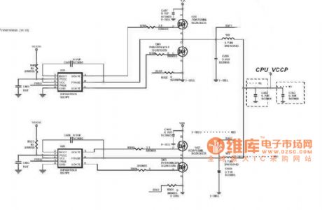
P4 power supply circuit diagram as shown (View)
View full Circuit Diagram | Comments | Reading(1816)
DUM23-48/300 Ⅱ dc power distribution unit electrical principle diagram
Published:2014/3/6 20:10:00 Author: | Keyword: DUM23-48/300 Ⅱ dc power distribution unit electrical principle diagram,
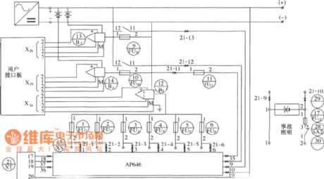
As shown in figure, B2 (13), B3 (14) for the hall current sensor; FU9 (9), FU10 (10) for the fuse; AP646 for fusing the alarm signal board; X24, X26 and X29 for user interface board of the terminal; XT for socket. (View)
View full Circuit Diagram | Comments | Reading(1762)
| Pages:2/291 1234567891011121314151617181920Under 20 |
Circuit Categories
power supply circuit
Amplifier Circuit
Basic Circuit
LED and Light Circuit
Sensor Circuit
Signal Processing
Electrical Equipment Circuit
Control Circuit
Remote Control Circuit
A/D-D/A Converter Circuit
Audio Circuit
Measuring and Test Circuit
Communication Circuit
Computer-Related Circuit
555 Circuit
Automotive Circuit
Repairing Circuit