
Alarm Control
Index 15
PRECISION_LIGHT_ACTIVATED_ALARM
Published:2009/6/14 22:55:00 Author:May
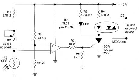
The light-sensitive CDS cell R8 conftgured In a bridge circuit with IC1 as a comparator causes IC1's output to go high when light strikes the CDS cell R8,triggering SCR1 This lights LED1 andturns on opto isolator IC2,which switches the load (View)
View full Circuit Diagram | Comments | Reading(1506)
LIGHT_ACTIVATED_ALARM_WITH_LATCH
Published:2009/6/14 22:55:00 Author:May
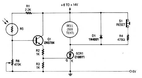
In this circuit, light causes R5 to conduct forward-biasing Q1. R6 sets sensitivity. SCR1 is triggered from the emitter voltage on LQ1, sounding the alarm bell. When 51 is depressed, SCR1 un-latches. Be sure that a self-interrupting alarm (electromechanical buzzer or bell) is used. (View)
View full Circuit Diagram | Comments | Reading(1181)
LIGHT_BEAM_ALARM_PREAMPLIFIER
Published:2009/6/14 22:53:00 Author:May
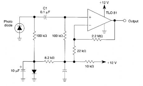
This circuit can be used for light beams to 20 kHz .The gain of the operational amplifier is set for a 40-dB gain. (View)
View full Circuit Diagram | Comments | Reading(1217)
DARK_ACTIVATED_ALARM_WITH_PULSED_TONE_OUTPUT
Published:2009/6/14 22:51:00 Author:May
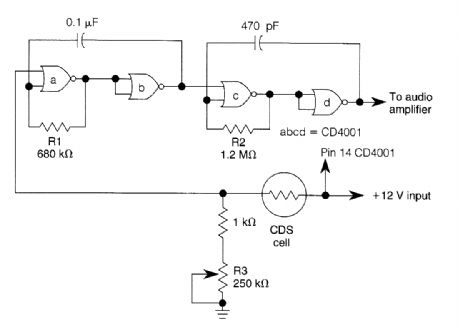
NOR gates a and b form a low-frequency oscillator that is activated when the CDS cell,underdark conditions,causes NOR gate ato see alogic zero at one input This low-frequency (10 Hz) gates a high-frequency oscillator (c and d) to oscillate at around 1000 Hz.R1 can be varied to change the pulse rate and R2 to change the tone.R3 sets the trigger point. (View)
View full Circuit Diagram | Comments | Reading(1826)
LIGHT_BEAM_ALARM_FOR_INTRUSION_DETECTION
Published:2009/6/14 22:46:00 Author:May
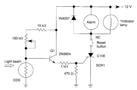
When the light beam that falls in the CDSphotocell is interrupted,transistor(EN3904) conducts thereby triggering SCR1 (C106) and activating alarm bell. S1 resets the SCR. The alarm bell should be a self-interrupttng electromechanical type. (View)
View full Circuit Diagram | Comments | Reading(2150)
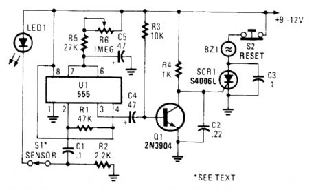
555_BASED_ALARM
Published:2009/6/14 22:43:00 Author:May
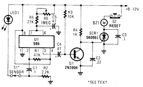

The alarm circuit has a single 555。scillator/timer(U1)performing double duty;serving both in the alarm-trigger circuit and the entry-delay circuit. In this application,the trigger mput of U1 at ptn 2 iS held high via R1,A normally-closed sensor switch,S1,supplies a positive voltage to the junction of R2 and C1,and lights LED1.With both ends of C1 tied high,there is no charge on C1 But when S1 opens,C1(initially acting as a short) momentarny pulls pm 2 of U1 low, triggering the timed delay circle At the beginning of the timing cycle,U1 produces a positive voltage at put 3,which charges FAUito near the positive voltage at put 3,which charges C4 to near the positive supply voltage Transistor Q1 is heavily biased on by R3,keeping its collector at near ground level With Qt on,SCR1’s gate lOclamped to ground,holding it off. When the delay circuit times out,pin 3 of U1 goes low and ties thepositive end of C4 to ground,That turns Q1 offWhen Q1 turns off,the voltage at the gate of SCR goes positive,turning on the SOP and sounding the alarm,The delay time is adjustable from just a few seconds(R6 set to its minimum resistance) to about one minute(R6 adjusted to its maximum resistance) (View)
View full Circuit Diagram | Comments | Reading(1087)
EXIT_DELAY_FOR_BURGLAR_ALARMS
Published:2009/6/14 22:16:00 Author:May
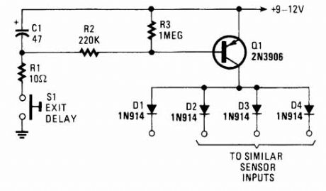
Depressing S1 charges C1 to the supply voltage. This biases Q1 on via bias resistors R2 and R3. A voltage is available for the duration of the delay period, to hold off the alarm circuit.C1 can be increased or decreased in value to al-ter the delay times. (View)
View full Circuit Diagram | Comments | Reading(1089)
PIEZOELECTRIC_ALARM
Published:2009/6/14 22:13:00 Author:May
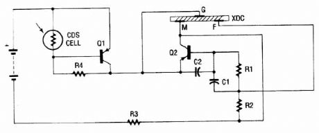
01,C2...............047 Disc Capacitor Q1,Q2.......... ... 2N3906 Transistor R1................ 6.8K Resistor R2..................33K Resistor R3................. 200 ohm Resistor R4..................75K Resistor XDC.................Piezoelectric transducer
The alarm uses a fixed-frequency piezoelectric buzzer in conjunction with the cadmium-sulfide (CDS) cell and the two-transistor circuit to provide a unique effect. Whenever light reaches the CDS photo-electric cell, the alarm is silent. But when no light strikes the cell, transistor Q1 tums on, and the circuit emits a high-pitched tone.The alarm consists of a piezoelectric disk that oscillates at the fixed frequency of 3. 137 kHz, cre-ated by transistor Q2, capacitor C1 and C2, and resistors R1 through R3. Transistor Q1 is used as a switch. It is forward-biased on by R4; however, the CDS cell turns Q1 off when the light is strik-ing it.A CDS photo cell is made from cadmium sulfide, a semiconductor material that changes resis-tance when the light strikes it. The greater the amount of light, the lower the resistance. The low re-sistance conducts positive voltage to the base of pnp transistor Q1, keeping it turned off' when the light shines on the CDS cell. As soon as the light is removed, the CDS cell provides a resistance of over 100 kQ. That causes Q1 to tum on, allowing a positive voltage to reach the emitter lead of Q2, which then begins to oscillate. That then causes the piezoelectric element (transducer) to produce a loud signal. (View)
View full Circuit Diagram | Comments | Reading(1325)
HEAT_OR_LIGHT_ACTIVATED_ALARM
Published:2009/6/14 22:06:00 Author:May
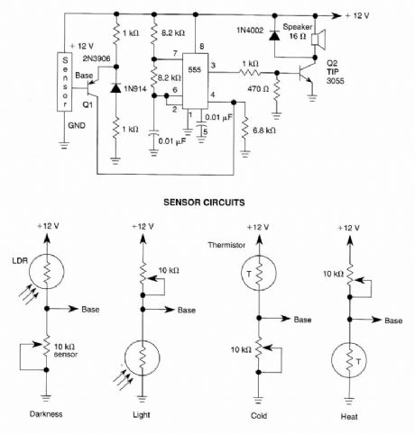
The tone generated by a 555 oscillator can be turned on (activated) by heat or light. That causes Q1 to conduct transistor W2 (TIP 3055).Q2 (TIP 3055) acts as an audio amplifier and speaker driver. (View)
View full Circuit Diagram | Comments | Reading(1775)
NO_DOZE_ALARM
Published:2009/6/14 22:00:00 Author:May
This circuit sends out a loud tone if the input switch(S2) is not retriggered at pre-set intervals. If you fall asleep and miss re-triggering the circuit, it will sound until you press S2. (View)
View full Circuit Diagram | Comments | Reading(923)
AUDIO_ALARM
Published:2009/6/14 21:59:00 Author:May
In the circuit, UI amplifies the audio picked up by the condenser microphone. Resistor RI limits current, while R2 and R3 center the output of the amplifier to 1/2 B+ to allow a singleended sup-ply to be used. Diodes Dl and D2 rectify the output of U1, and C3 filters the resulting pulsing dc.Thus, a dc voltage that is proportional to the ambient sound level is produced.That voltage is presented to the noninverting input of U2. The inverting input is provided with a reference voltage of between 0 and 1/2 B+, which is set by R11.As long as the noise level is low enough to keep the voltage at pin 3lower than the voltage at pin 2, the output of U2 stays low (approximately 1V). That is enough to bias Q1 partially on. A voltage divider, formed by R8/RIO and Q1 (when it's partially on), prevents Q2 from turning on.When the noise level is high enough to bring the voltage at pin 3 higher than the voltage at pin 2, the output of U2 goes high. That turns Q1 fully on and drives Q2 into saturation. The piezo buzzer then sounds until the power is cut off. (View)
View full Circuit Diagram | Comments | Reading(898)
CLOSED_LOOP_ALARM
Published:2009/6/14 21:40:00 Author:May
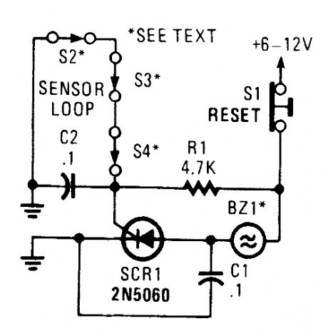
A string of three series-connected, normally closed switches are connected across the gate of an SCR. When one opens, the SCR triggers via R1, sounding an alarm. The alarm should be of the noninterrupting type. (View)
View full Circuit Diagram | Comments | Reading(1032)
WARBLE_ALARM
Published:2009/6/14 21:50:00 Author:May

This circuit uses a 556 to first generate a low frequency square wave, that is modulated to pro-duce two alternate tones of about 400 and 500 Hz. Circuit generates warble alarm of European emer-gency vehicles. The frequencies of the oscillators are determined by the values of R1, C1 and R2, C2. (View)
View full Circuit Diagram | Comments | Reading(971)
DELAYED_ALARM
Published:2009/6/14 21:42:00 Author:Celina
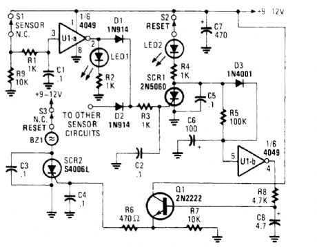
The alarm/sensor circuit shown is built around two SCRs, a transistor, a 4049 hex inverter, and a few support components, all of which combine to form a closed-loop detection circuit with a delay feature. The delay feature allows you to enter a protected area and deactivate the circuit before the sounder goes off.Assuming that the protected area has not been breached (i.e., S1 is in its normally-closed posi-tion), when power is first applied to the circuit, a positive voltage is applied to the input of UI-a through 51 and RI, causing its output to go low. That low is applied to the gate of SCR1, causing it to remain off. At the same time, C6 rapidly charges toward the +Tsupply rail through S2, LED2, R4, and D3. The charge on C6 pulls pin 5 of UI-b high, causing its output at pin 4 to be low. That low is ap-plied to the base of Q1, keeping it off. Because no trigger voltage is applied to the gate of SCR2 (via Q1), the SCR remains off and BZ1 does not sound.But should S1 open, the input of UI-a is pulled low via R9, forcing the output of UI-a high, light-tng LED1. That high is also applied to the gate of SCR1 through Dl and R3, causing SCR1 to turn on.With SCR1 conducting, the charge on CG decays, the input of UI-b at pin 5 is pulled low, forcing its output high, slowing charging C8 through R8 to a voltage slightly less than the positive supply rail.Transistor Q1 remains off until C8 has charged to a level sufficient to bias Q1 on, allowing suffi-cient time to enter the protected area and disable the alarm before it sounds. Once C8 has developed a sufficient charge, Ql turns on and supplies gate current to SCR2 through R6, causing the SCR to turn on and activate BZ1. If the circuit is reset before the delay has timed out, no alarm will sound.The delay time can be lengthened by increasing the value of either or both C6 and R5; decreas-tng the value of either or both of those components will shorten the delay time.All of the switches used in the circuit are of the normally-closed (NC) variety. Switch 51 can be any type of NC security switch. Switch 52 can be either a pushbutton or toggle switch. Because 53 is used to disable the sounder (BZl) only, anything from a key-operated security switch to a hidden toggle switch can be used. (View)
View full Circuit Diagram | Comments | Reading(1349)
Water Activated Alarm
Published:2011/7/24 22:33:00 Author:Ecco | Keyword: Water Activated Alarm
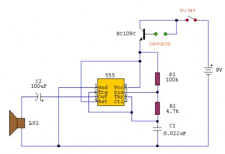
The circuit uses a 555 timer wired as an astable oscillator and powered by the emitter current of the BC109C. Under dry conditions, the transistor will have no bias current and be fully off. However as the probes get wet the transistor will conduct and sounding the alarm.An On/Off switch is provided and remember to use a non-reactive metal for the probe contacts. Gold or silver plated contacts from an old relay may be used, however a cheap alternative is to wire alternate copper strips from a piece of veroboard. These will eventually oxidize over but as very little current is flowing in the base circuit, the higher impedance caused by oxidization is not important. No base resistor is necessary as the transistor is in emitter follower, current limit being the impedance at the emitter (the oscillator circuit). (View)
View full Circuit Diagram | Comments | Reading(1)
The gas limiting alarm mining lamp circuit diagram 3
Published:2011/7/14 20:40:00 Author:Lucas | Keyword: Gas limiting, alarm , miners lamp
The gas limiting alarm miner's lamp circuit is composed of the gas detection circuit, electronic switch circuit and audio alarm circuit, and the circuit is shown as the chart. The gas detection circuit is composed of the resistor R1, potentiometer RP and gas sensor. Electronic switch circuit is composed of the thyristor VT and RP. Audio alarm sound is composed of the integrated circuit IC, resistor R2, transistor Ⅴ and speaker BL. R1 and R2 use 1/4W carbon film resistors or metal film resistors. C selects select aluminium electrolytic capacitors with the voltage in 6.3V. V uses 59013 or 3DG12 NPN silicon transistor. VT uses MCR100-6 or BTl69 thyristor.
(View)
View full Circuit Diagram | Comments | Reading(769)
The gas limiting alarm mining lamp circuit diagram 2
Published:2011/7/14 20:40:00 Author:Lucas | Keyword: Gas limiting , alarm , miners lamp
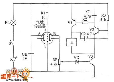
The gas limiting alarm miner's lamp circuit is composed of the gas detection circuit, controlled oscillator circuit and lighting circuit, and the circuit is shown as the chart. Gas detection circuit is composed of the gas sensor, resistor R1 and potentiometer RP. Controlled oscillator circuit is composed of the potentiometer RP, diode VD, transistors V1 ~ V3, resistors R2 and R3, capacitors C1 and C2 and the relay K. Lighting circuit is composed of the battery GB, light EL, light switch S and the normally closed contact of K. The miner's lamp EL is lit by turning on the light switch S, . R1 ~ R3 select 1/4W metal film resistors. RP uses small synthetic carbon potentiometer or variable resistor. C1 and C2 select aluminium electrolytic capacitors with the voltage in 6.3V.
(View)
View full Circuit Diagram | Comments | Reading(1141)
Body induction alarm circuit
Published:2011/5/12 22:31:00 Author:Nicole | Keyword: body induction, alram
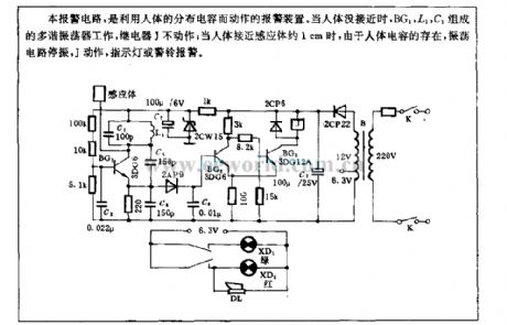
This alarm circuit uses the body distributed capacitance to make a alarm device. When there is nobody closing, BG1, L1, C1 form a multivibrator, relay J is not working; when people are closing the inductor about 1cm, because of the body capacitance, the oscillation circuit will stop vibrating, J starts to work, then the indicator light or warning bellwill alarm. (View)
View full Circuit Diagram | Comments | Reading(1024)
CPU fan stopping alarm circuit diagram
Published:2011/6/24 4:17:00 Author:Ecco | Keyword: CPU , fan , stopping alarm

D1 and D2 are respectively the infrared transmitter and infrared receiver tubes, and they are against the installation and 1.2-1.8 cm apart. When it gets power, D1 emits a continuous infrared beam IR, which is intermittently hitting the receiver tube under the block of blade from time to time. This, V1 will have a pulse type of bias current to make the two ends of R2 generate pulse voltage. D4 must use a germanium diode such as 1N60, 2AP9 and so on. SPEAKER can select the type on the quartz clock with pointer.
(View)
View full Circuit Diagram | Comments | Reading(1633)
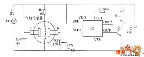
The gas limiting alarm miner lamp circuit diagram 1
Published:2011/7/6 22:06:00 Author:Lucas | Keyword: Gas limiting, alarm , miners lamp
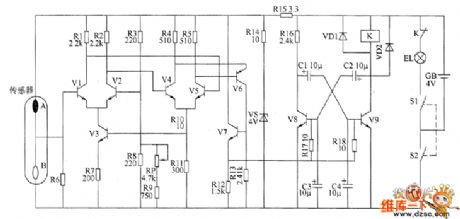
The gas limiting alarm miner's lamp circuit is composed of the detection amplifier circuit, and the circuit is shown as the chart. RP uses synthetic carbon potentiometer. C1 ~ C4 select aluminium electrolytic capacitor with the withstang voltage being more than 6.3V. VD1 and VD2 use 1N4007 or 2CP22 silicon rectifier diodes. VS selects 2CW11 silicon regulator diode. V1 ~ V5 and V7 select 59013 or 3DK4 silicon NPN transistors; V6 uses 59012 or 3CG21 silicon PNP transistor; V8 and V9 select 58050 silicon NPN transistors. K uses 4099 or JRC-5M DC relay. The sensor uses carrier catalytic gas sensor. Power switch S, miner's lamp EL, battery CB are the accessories of the original miner's lamp.
(View)
View full Circuit Diagram | Comments | Reading(692)
| Pages:15/18 123456789101112131415161718 |
Circuit Categories
power supply circuit
Amplifier Circuit
Basic Circuit
LED and Light Circuit
Sensor Circuit
Signal Processing
Electrical Equipment Circuit
Control Circuit
Remote Control Circuit
A/D-D/A Converter Circuit
Audio Circuit
Measuring and Test Circuit
Communication Circuit
Computer-Related Circuit
555 Circuit
Automotive Circuit
Repairing Circuit