
Index 235
Double-connection double-control switch circuit
Published:2011/5/8 5:37:00 Author:TaoXi | Keyword: Double-connection, double-control, switch
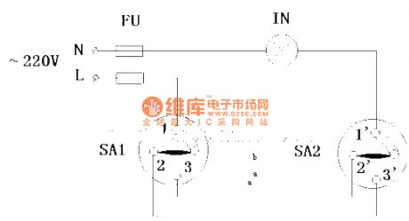
The Double-connection double-control switch circuit is as shown:
(View)
View full Circuit Diagram | Comments | Reading(645)
DC/DC converter of chaing 5V to ±15V Circuit
Published:2011/5/7 6:17:00 Author:Joyce | Keyword: DC/DC , converter of, chaing 5V to ±15V
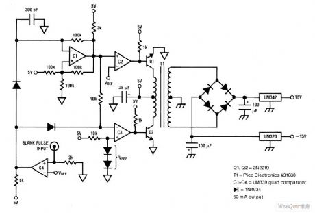
DC/DC converter of chaing 5V to ±15V Circuit (View)
View full Circuit Diagram | Comments | Reading(2867)
Snore Sensing Circuit
Published:2011/5/6 6:11:00 Author:Sue | Keyword: Snore, Sensing
View full Circuit Diagram | Comments | Reading(489)
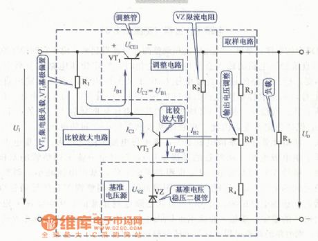
Voltage Stabilizing Circuit with Amplifying Transistor
Published:2011/5/6 6:13:00 Author:Sue | Keyword: Voltage Stabilizing, Amplifying Transistor
View full Circuit Diagram | Comments | Reading(477)
Principle of 60V Circuit
Published:2011/5/6 0:54:00 Author:Sue | Keyword: Principle, 60V
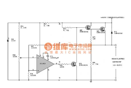
View full Circuit Diagram | Comments | Reading(536)
Single Supply RTD Amplifying Circuit
Published:2011/5/6 6:02:00 Author:Sue | Keyword: Single Supply, RTD, Amplifying
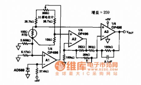
Sensor and OP196/296/496 type battery positive/negative input/output operational amplifier circuit.
Application: It is used in sensor adjustment, small power control, small-sized apparatus, battery monitoring and so on.
(View)
View full Circuit Diagram | Comments | Reading(1350)
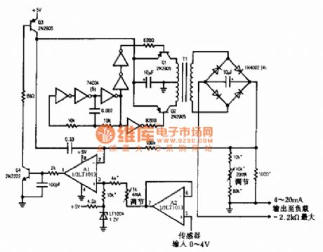
4-20MA Current Transmitter Circuit with 5V Power
Published:2011/5/6 6:02:00 Author:Sue | Keyword: 4-20MA, Current, Transmitter, 5V Power
View full Circuit Diagram | Comments | Reading(733)
Timing Nicel Cadmium Battery Charger(CD4060) Circuit
Published:2011/5/6 5:50:00 Author:Sue | Keyword: Timing, Nicel Cadmium, Battery, Charger

View full Circuit Diagram | Comments | Reading(2456)
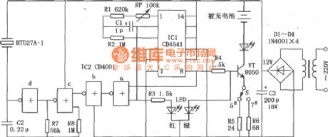
Nicel Cadmium Battery Charger Circuit Composed of CD4541
Published:2011/5/6 5:49:00 Author:Sue | Keyword: Nicel Cadmium, Battery, Charger
View full Circuit Diagram | Comments | Reading(1233)
Nicel Cadmium Battery Charger(LM393) Circuit
Published:2011/5/6 5:47:00 Author:Sue | Keyword: Nicel Cadmium, Battery, Charger
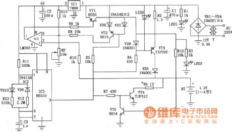
View full Circuit Diagram | Comments | Reading(3567)
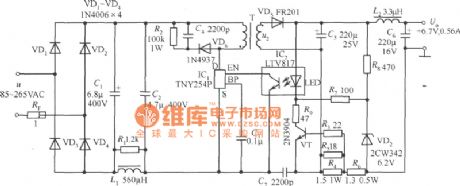
Mobile Phone Battery Constant Current Charger(TNY254P +6.7V、0.56A) Circuit
Published:2011/5/6 5:45:00 Author:Sue | Keyword: Mobile Phone, Battery, Constant Current, Charger
View full Circuit Diagram | Comments | Reading(753)
Current-limiting Step-down Resistance and Capacitance Storage Battery Charger Circuit
Published:2011/5/6 5:40:00 Author:Sue | Keyword: Current-limiting, Step-down, Resistance, Capacitance, Storage Battery, Charger
View full Circuit Diagram | Comments | Reading(557)
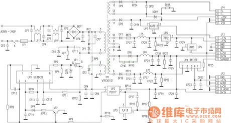
Amoi DVD Power(UC3842) Circuit
Published:2011/5/6 2:06:00 Author:Sue | Keyword: Amoi, DVD, Power
View full Circuit Diagram | Comments | Reading(3396)
No polar electrolysis capacitor aging circuit diagram
Published:2011/5/5 3:31:00 Author:Crystal Liu | Keyword: no polar electrolysis capacitor, aging circuit
No polar electrolysis capacitor refined circuit. (View)
View full Circuit Diagram | Comments | Reading(540)
Application circuit diagram of simplified VMOS switching power supply
Published:2011/5/5 7:27:00 Author:Nicole | Keyword: switching power supply, VMOS
VMOS switching power supply circuit diagram. Because of adopting voltage comparator 710, so the circuit issimpler than former. As shown, resistor R1, R2, R3 and regulator VDl, VD2 form divider regulator circuit, three groups of 5V, 6V and 18V are separated from 28V input voltage,they areused as the power supply; resistors R12, R13, capacitor C13, diodes VD6, VD7 and transistor VT3 constitute the power soft-start circuit. The moment of power turn on, the drive pulse width of VMOS tube VTl increases exponentially. when the comparator 710 cut off the drive pulse firstly, it can prevent the current of energy storage inductor too large. When the switch VTl cut down, the output voltage of switching power supply continues to rise because the current of energy storage inductor L1 still charge to the output filter capacitor C6 ~ C12. In other words, soft-start circuit make the current of energy storage inductor L1 rise slowly when the power supply start working, then to prevent output voltage from large overshoot. After the power supply into steady-state, the soft-start circuit is not work.
(View)
View full Circuit Diagram | Comments | Reading(1234)
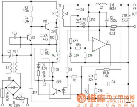
Separate excitation switching power supply circuit diagram using free-running multivibrator as pulse generator
Published:2011/5/5 7:32:00 Author:Nicole | Keyword: switching power supply, multivibrator, pulse generator
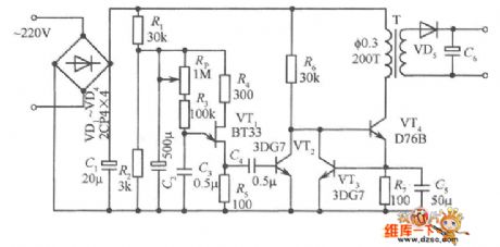
As shown, VTlis the switch; VT2, VT3is push tube; VT4 is emitter follower. Separate excitation oscillation circuit is undertaken by free-running multivibrator which composed of VT5, VT6, C2, C3, R3, R4. VT7, VT8 form emitter-coupled differential amplifier to be used as the error amplification. Sampling circuit consists of resistors R7, R8 and in series with potentiometer R9. Voltage reference circuit is made of regulator diode VD4 and R5. Diode VDl, VD2 is used to prevent reverse voltage breakdown the push tube VT2, VT3 emitter. VD3 for the freewheeling diode; L for the energy storage inductor.
The turn on/off of switch regulator is flipped by multivibrator, and controlled by emitter follower VT4. The flip time of multivibratoris determined by the error amplifier. In other words, The flip time of VT5 from the end to turnare decided by the current of VT8 charge to C3. The current of VT8 is larger, the deadline of VT5 is longer. Similarly, the flip time of VT6 from the end to turn is decided by the current of VT7 charge to C2. The current of VT7 is larger, the deadline of VT5 is shorter. When the output voltage isdropped for some reason, VT8 tube collector current of the differential amplifier decreases, tube collector current of VT7increases, so the conduction time of VT5 is shortened, and extended the deadline, leading to the longerconduction time of VT4 longer, the cut-off shorter, and ultimately the conduction time of control switch tubeis lengthening, the deadline is shortening,so that the output voltage to rise, remain the stability of output voltage.
(View)
View full Circuit Diagram | Comments | Reading(1489)
Electric Bicycle Storage Battery Charger(UC3842) Circuit
Published:2011/5/6 0:52:00 Author:Sue | Keyword: Electric Bicycle, Storage Battery, Charger
View full Circuit Diagram | Comments | Reading(3099)
MC3406A buck-boost DC-DC convertor integrated circuit diagram
Published:2011/5/5 7:32:00 Author:Nicole | Keyword: Integrated convertor
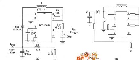
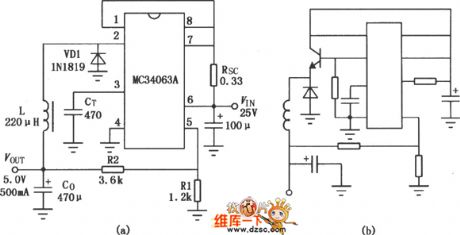
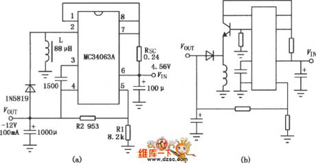
MC3406A is a new monolithic buck-boost DC-DC converter integrated circuit, the input voltage is 3 ~ 40V, output voltage isadjustable, the output switch current can up to l. 5A, and it hasa temperature compensated voltage reference, it has the function of current limit. The IC is equipped with only a few external components, then it can form boost, buck, anti-transition DC-DC converter, it can be widely used in various portable instruments, meters and so on.
MC3406A used as boost DC-DC convertor circuit:
MC3406A used as buck DC-DC convertor circuit:
MC3406A used as anti-transition DC-DC convertor circuit:
(View)
View full Circuit Diagram | Comments | Reading(3564)
Switch Power Charger Circuit
Published:2011/5/6 0:52:00 Author:Sue | Keyword: Switch Power, Charger
View full Circuit Diagram | Comments | Reading(637)
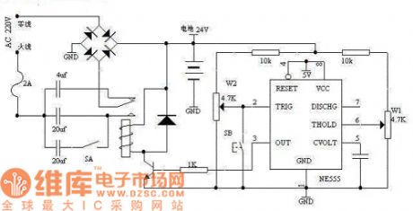
Timed street light circuit with light control
Published:2011/5/5 7:49:00 Author:Nicole | Keyword: timed street light, light control
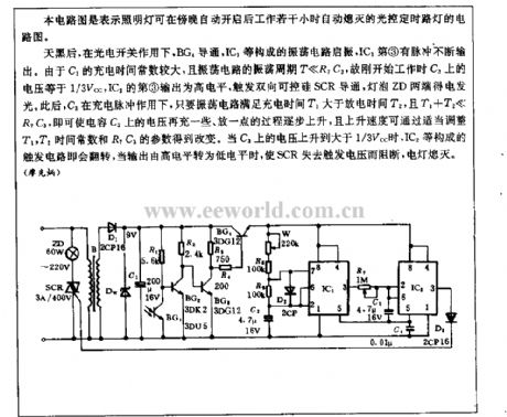
It is an optical control timing street lamp circuit diagram, at night-fall the floodlight will automatically turn on, after a few hours later, it can automatically turn off.
After dark, by the action of photoelectric switch, BG4 turns on, the oscillation circuit composed of IC1 starts to oscillate, ③ pulse constantly output. Because the charge time constant is larger, and the oscillation period T< (View)
View full Circuit Diagram | Comments | Reading(1166)
| Pages:235/291 At 20221222223224225226227228229230231232233234235236237238239240Under 20 |
Circuit Categories
power supply circuit
Amplifier Circuit
Basic Circuit
LED and Light Circuit
Sensor Circuit
Signal Processing
Electrical Equipment Circuit
Control Circuit
Remote Control Circuit
A/D-D/A Converter Circuit
Audio Circuit
Measuring and Test Circuit
Communication Circuit
Computer-Related Circuit
555 Circuit
Automotive Circuit
Repairing Circuit