
Index 236
Photoelectric switch circuit in AC network
Published:2011/5/5 7:53:00 Author:Nicole | Keyword: photoelectric switch, AC network
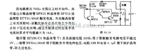
When the light intensity is more than 700lx, this circuit will take action. The light-sensitive transistor BPX25 and transistor BFY52 provide SCR BTY91/800R with trigger current. When the light-sensitive transistor has light, this trigger pulse always appears about 6°behind each positive half cycle starting point, the maximum arithmetic mean value of DC half wave current flows load is 16A.
The regulator tube BZY88/C5 and transistor T1, the connected resistance 390Ω are used to limit trigger circuit voltagenomore than 6V. Diode BYX45/800R is used to break negative half cycle network voltage, the resistance 33Ω and capacitance 0.1μF are used to protect SCR, it can prevent overvoltage. (View)
View full Circuit Diagram | Comments | Reading(668)
Simple and special regulator circuit
Published:2011/5/5 7:52:00 Author:Nicole | Keyword: regulator
In some cases, if a regulated power supply is required for controlling and detecting purpose in service. Then the circuir is very simple and convenient.
To adjust the ratio of R1, R2, one can change the input voltage of steady voltage unit, the C1 is related to the load of output steady voltage.
(View)
View full Circuit Diagram | Comments | Reading(637)
Optical transmission detection circuit
Published:2011/5/5 7:51:00 Author:Nicole | Keyword: optical transmission detection circuit
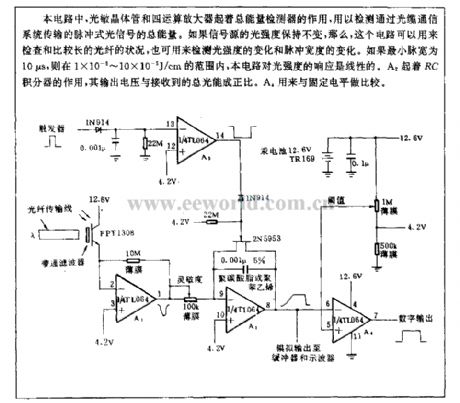
In this circuit, phototransistor and four operational amplifier take the action of total energy detector, to detect the total energy of pulse optical transported by the optical cable communication system. If the light intensity of singal source remains the same, then this circuit can be used to test and compare the situation of optical fiber, it also can be used to detect the change of light intensity and pulse width. If the minimum pulse width is 10μs, then the response of this circuit to light intensity is linear. A2 has the function ofRC integrator, the output voltage is directly proportional to the total received light energy. A4 is used to compare with the fixed level. (View)
View full Circuit Diagram | Comments | Reading(2042)
Travel Charger(Ericsson 788) Circuit
Published:2011/5/6 0:36:00 Author:Sue | Keyword: Travel Charger, Ericsson 788
View full Circuit Diagram | Comments | Reading(701)
Simplified Charger Circuit Composed of STD 9732
Published:2011/5/6 0:43:00 Author:Sue | Keyword: Simplified, Charger
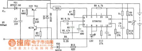
View full Circuit Diagram | Comments | Reading(554)
Battery Charger Circuit Composed of MIC5158
Published:2011/5/6 0:41:00 Author:Sue | Keyword: Battery Charger
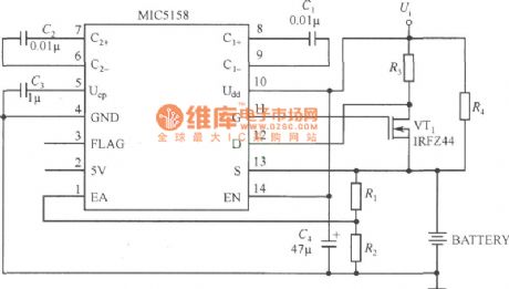
View full Circuit Diagram | Comments | Reading(620)
Charger(Walkman)Circuit
Published:2011/5/6 0:33:00 Author:Sue | Keyword: Charger, Walkman,
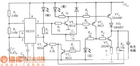
View full Circuit Diagram | Comments | Reading(1066)
Benq Laptop Battery Charger Circuit
Published:2011/5/6 0:29:00 Author:Sue | Keyword: Benq, Laptop, Battery, Charger
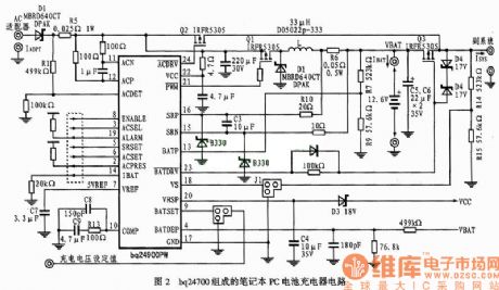
View full Circuit Diagram | Comments | Reading(2673)
Dual Stabilized Voltage Output Circuit
Published:2011/5/6 0:32:00 Author:Sue | Keyword: Dual, Stabilized Voltage, Output
View full Circuit Diagram | Comments | Reading(648)
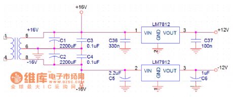
Drive display circuit with multi-channel turn mending method
Published:2011/4/19 7:08:00 Author:Nicole | Keyword: multi-channel, turn mending method, drive display
This circuit uses battery powered. It makes an encode driver to drive LEDs of MAN-4 display one by one through multi-channel transit way, then to reduce the power consumption of battery. Because the reading which people seen is still have impression in whole display cycle, so the display seem to display continuously. The peak current of display is 20mA, the test duration of each LED only accounts for 12.5% of the whole display cycle. Four MC1402/8 FCSR, to latch the value which is form MC14518 count chain,then itaccomplishes the multi-channel transit function. (View)
View full Circuit Diagram | Comments | Reading(623)
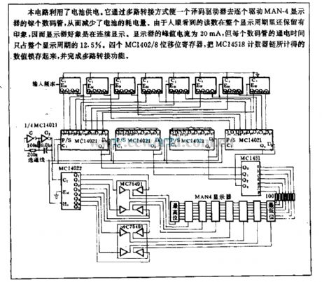
Integrated regulated power supply with overvoltage protection composed of CW137
Published:2011/5/5 8:11:00 Author:Nicole | Keyword: regulated power supply, overvoltage protection
Integrated regulated power supply with overvoltage protection composed of three terminal adjustable negative output voltage integrated regulator CW137.
When R1=250Ω, R2=6Ω, it is changeable, Ci=1μF, Co=1μF Ta capacitor, CAdj=10μF, VD1 and VD2 are 1N4002, Uo=1.25~32V. (View)
View full Circuit Diagram | Comments | Reading(555)
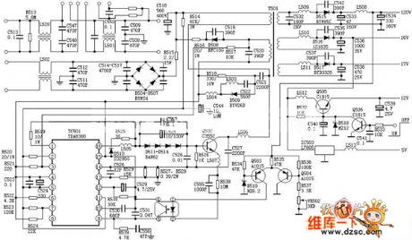
Jinxing C7458 Switching Power Supply Circuit
Published:2011/5/5 9:48:00 Author:Felicity | Keyword: Switching Power Supply Circuit,
The picture above shows Jinxing C7458 Switching Power Supply Circuit. (View)
View full Circuit Diagram | Comments | Reading(1045)
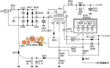
Separate-excited Single-ended Flyback Switching Power Supply 4C7108 Circuit
Published:2011/5/5 9:49:00 Author:Felicity | Keyword: Separate-excited Single-ended Flyback Switching Power Supply Circuit,
The picture above shows the stimulated single-ended flyback switching power supply 4C7108 circuit. (View)
View full Circuit Diagram | Comments | Reading(1193)
Panasonic M12H Switching Power Supply Circuit
Published:2011/5/5 9:52:00 Author:Felicity | Keyword: Panasonic, Switching Power Supply Circuit,
The picture above shows the Panasonic M12H Switching Power Supply Circuit. (View)
View full Circuit Diagram | Comments | Reading(1019)
PQl2RF2 controllable voltage regulator integrated circuit diagram
Published:2011/5/5 9:49:00 Author:Rebekka | Keyword: Controllable voltage regulator integrated circuit
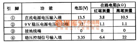
PQ12RF2 is a controllable voltage regulator integrated circuit. It is widely used in equipment such as species of large screen color TV in the liver. PQ12RF2 integrated circuit IC uses 4-pin single row package, the pin functions and data of the integrated circuit are listed in table 1. (View)
View full Circuit Diagram | Comments | Reading(623)
0-1 hours of power supply timing AC power supply circuit diagram
Published:2011/5/5 22:08:00 Author:Rebekka | Keyword: power supply timing AC power supply
View full Circuit Diagram | Comments | Reading(478)
Based on a pulse regulating neon type switching regulated power supply circuit diagram
Published:2011/4/22 18:53:00 Author:Nicole | Keyword: switching power supply
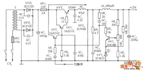
This is a pulse Ni switching power supply circuit diagram, it is Kaige 4D17U produced by radio four factory in Shanghai. The power supply of 35cm black and white TV.
The main technical indicators are as follows: Output voltage: 12V; Output Current: 1A; power consumption <20W; efficiency> 64%; resistance <0.075Ω; ripple <15mV; mains voltage: 160 ~ 240V.
As shown, 6VDl, 6VD2 form full-wave rectifier circuit; 6C3is filter capacitor; 6C1, 6C2 are used to weaken the inrush current; 6VT7, 6VT2, 6VT3 and 6R4, 6C9 constitute the self-excited multivibrator, 6VT7 also is the switching tube.
When the 12V output voltage decreases for some reason, the base of error amplification 6VT5 obtain the voltage from the sampling circuit 6R6, 6R9, 6R8 also drop, the collector voltage of 6VT5 rises, potential base 6VT3 increases, the output pulse of switch controls tube 6VT7 widen, then the reducing voltage rises again. On the contrary, to adjust on the opposite by the above process when the output voltage goes down, to make the output voltage stable.
(View)
View full Circuit Diagram | Comments | Reading(2043)
Strong stability boost output circuit diagram
Published:2011/4/7 3:44:00 Author:Nicole | Keyword: boost, output
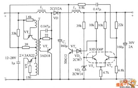
The figure is a boost output type practical circuit. VT3 is the switching regulator; regulator VD2 can change the potential; VT4 is inverting isolation amplifier; Ui is divided by the VT4 and its 33kΩ load resistor. The two voltage supply for pulse generator circuit. Pulse generator circuit consists of the transformer T and VTl, VT2. This is a non-symmetric transformer feedback self-excited multivibrator. The supply of VTl is from the voltage of 33kΩ load resistor, and the current of resistance depends on the current of VT4. VT1, VT2 have different supply voltage, the oscillation amplitude of half and half weeks is changed in direct proportion, the width is inversely proportional to the change, to control the on and off time of VT3. When the output voltage increases, the differential pair VT6 current of error amplifier increases, VT5 current decreases, the collector potential rise, VT4 current increases, 33kΩ resistor voltage drop increases, VTl pipe supply pressure is increased, conduction time is shortened, the conduction time of switch VT3 is shortened, too.
The circuit input voltage is 12 ~ 28V, the output can be stable for 30V, maximum output power is 60W, efficiency is 89.4% ~ 94.7%, instability is ± 0.33%, the ripple coefficient of output voltage is 0.02%, operating frequency is 10kHz.
(View)
View full Circuit Diagram | Comments | Reading(899)
Ring-type switching power supply constant current drive circuit diagram
Published:2011/3/30 3:29:00 Author:Nicole | Keyword: switching power supply, constant current drive
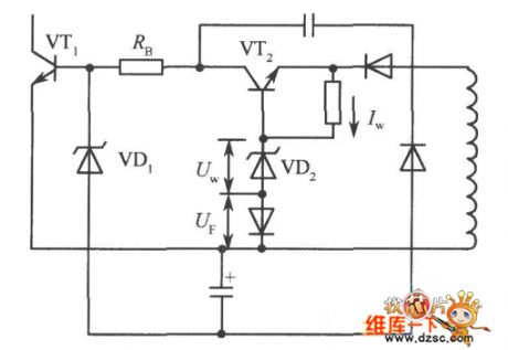
It is essentially a simple series regulator. The load is a fixed resistor RB. Even if the input voltage Ui changes, the current flowing through RB is constant. This will not only significantly reduce the loss of the resistance, but also to prevent intermittent oscillation. AC is in range of 100 ~ 200V, the power can work continuously.
In the ring-type switching power supply, the loss of the drive circuit of supply switching transistor base current is considerable. In addition to ensuring the switching transistor can fully turn with the minimum input voltage, the voltage UB on the transformer winding is in direct proportion to the input voltage Ui. when Ui rises, the drive current Id increases too, and the incremental losses of the base resistance Rb, can increase with the square of increasing part of Id.
When the drive current ID is increasing, the current of the branch of regulator diode must be increased, it may cause oscillation, that is, the switching works in a period of time, but will stop working in the adjacent time. Over and over again, the frequency of oscillation is about several hundred to several thousand Hertz.
To solve these problems, that is, when the input voltage changes, it can adopt constant current drive to remain drive current unchanged, as shown below.
(View)
View full Circuit Diagram | Comments | Reading(961)
Tiny intensity light control switch circuit
Published:2011/5/2 6:32:00 Author:Nicole | Keyword: light control switch
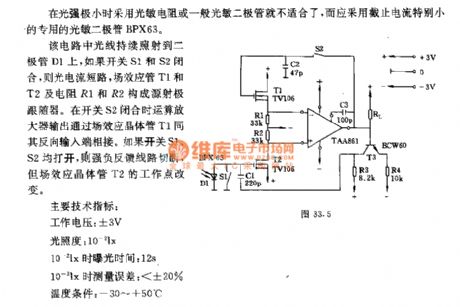
When the light intensity is tiny, it is unfit for adopting photosensitive resistance or general photodiode, it should use special photodiode BPX63 with small cut-off current.
In the circuit, the light constantly shines diode D1, if switches S1 and S2 is closed, then the photocurrent is short-circuited, the source emitter follower is composed of FETs T1 and T2, resistances R1 and R2. When switch S2 is closed, opertional amplifier output is connected to its inverting input terminal by FET T1. If switches S1 and S2 are all open, then the strong negative feedback is cut off, but the work point of FET T2 is changed.
Main technique target: work voltage: ±3V; illuminance: 0.01lx; the exposure time of 0.02lx: 12s; the measurement error of 0.01lx: < ±20%; temperature condition: -30~+50℃. (View)
View full Circuit Diagram | Comments | Reading(606)
| Pages:236/291 At 20221222223224225226227228229230231232233234235236237238239240Under 20 |
Circuit Categories
power supply circuit
Amplifier Circuit
Basic Circuit
LED and Light Circuit
Sensor Circuit
Signal Processing
Electrical Equipment Circuit
Control Circuit
Remote Control Circuit
A/D-D/A Converter Circuit
Audio Circuit
Measuring and Test Circuit
Communication Circuit
Computer-Related Circuit
555 Circuit
Automotive Circuit
Repairing Circuit