
Oscillator Circuit
Index 5
Pulse oscillator with adjustable duty cycle and frequency
Published:2013/2/18 2:11:00 Author:Ecco | Keyword: Pulse oscillator, adjustable duty cycle , frequency
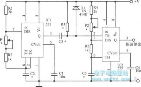
Pulse oscillator with adjustable duty cycle and frequency is shown as figure.
(View)
View full Circuit Diagram | Comments | Reading(1550)
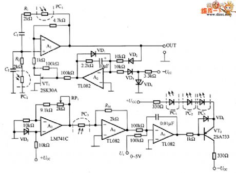
Variable pitch multivibrator circuit diagram
Published:2013/1/31 0:44:00 Author:Ecco | Keyword: Variable pitch, multivibrator
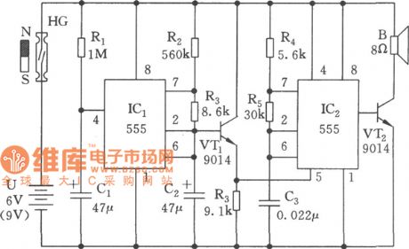
This circuit is composed of two 555 time-base circuits, and it can issue 400 ~ 2500Hz oscillatory wave with continuous changes, it is similar to the sound of public security police vehicles. The circuit consists of the boot delay, low-frequency oscillator and modulated tone generator.
(View)
View full Circuit Diagram | Comments | Reading(1322)
High-stability Wien bridge oscillator circuit
Published:2013/1/30 1:46:00 Author:Ecco | Keyword: High-stability , Wien bridge , oscillator

View full Circuit Diagram | Comments | Reading(1243)
Keying freedom multivibrator circuit
Published:2013/1/30 1:47:00 Author:Ecco | Keyword: Keying freedom multivibrator

Keying freedom multivibrator circuit is shown as figure.
(View)
View full Circuit Diagram | Comments | Reading(911)
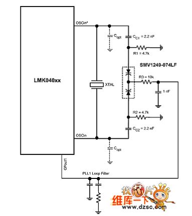
LMK04000 reference design schematics with crystal oscillator
Published:2013/1/29 2:26:00 Author:Ecco | Keyword: reference design , crystal oscillator
View full Circuit Diagram | Comments | Reading(901)
8 ~ 12MHz voltage controlled oscillator circuit diagram with stable output amplitude
Published:2012/12/21 1:44:00 Author:Ecco | Keyword: 8 ~ 12MHz , voltage controlled oscillator , stable output amplitude

In the circuit, VT2 controls the collector current of VT1, therefore, the oscillation amplitude of VT1 is very stable. VT4 output signal is converted into a DC signal by VD2 detector, here is the automatic gain controlling state, so that the DC voltage is kept constant. RP1's midpoint voltage is - 0.6V, and the current holding in R1 and R2 is equal, thereby controlling the output amplitude constant value. Oscillation frequency is decided by L1, C2, varactor diode VD1 and distributed capacitor. Uo output voltage is 2V, the frequency is 8 ~ 12MHz signal.
(View)
View full Circuit Diagram | Comments | Reading(1730)
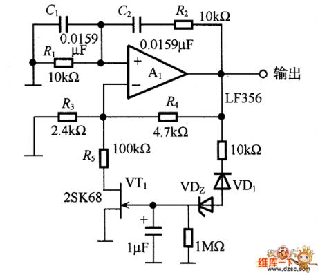
Low distortion Wien bridge oscillator circuit diagram
Published:2012/12/21 3:08:00 Author:Ecco | Keyword: Low distortion , Wien bridge, oscillator
The oscillation principle is that when the loop phase shift amount is an integer multiple of 0 ° or 360 °, the loop gain is greater than 1, the circuit starts oscillation. If the oscillation is increased, the circuit will be saturated, therefore it needs an amplitude stabilization circuit. In the circuit, the amplitude stabilization circuit uses a junction FET (VT1) drain - source resistor to connect with R1 in series to make R2 / 2 = 4.7kΩ / 2 = 2.35kΩ.
(View)
View full Circuit Diagram | Comments | Reading(2514)
Scanning oscillator circuit diagram
Published:2012/12/17 3:42:00 Author:Ecco | Keyword: Scanning oscillator
This circuit is composed of RC Wien bridge oscillator and voltage controlled resistor, wherein the Wien bridge circuit is available for RC circuit with a selected frequency, and A1 magnification is about three times, loop gain is 1. The output of A2 is half wave rectified by VD2, then it is comparing with the reference current generated by VD4 to make integrating, thereby controlling the VT1's gate voltage and changing the resistance between the drain - source.
(View)
View full Circuit Diagram | Comments | Reading(1144)
The PLL synthesized oscillator circuit diagram
Published:2012/11/11 20:16:00 Author:Ecco | Keyword: PLL , synthesized oscillator
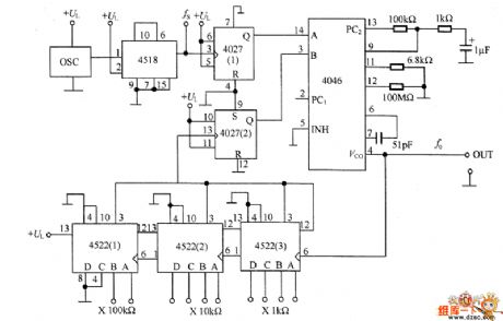
PLL synthesizer oscillator circuit is a feedback loop composed of reference oscillator, phase comparator, loop filter, voltage controlled oscillator, programmable frequency divider and other components. In the circuit, the reference oscillator uses a crystal oscillator (OSC) to output 1MHz or l00kHz 1/1000 or 1/100 divider and generate 1kHz signal, then it is compared with the output of 1 / N sub- frequency circuit. 4046 contains PC1 and PC2 two-phase comparators which can obtain the output corresponding to phase difference or frequency.
(View)
View full Circuit Diagram | Comments | Reading(5797)
The oscillator circuit diagram composed of crystal inverter
Published:2012/11/11 21:19:00 Author:Ecco | Keyword: oscillator , crystal inverter
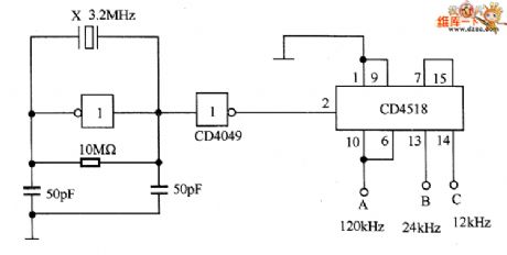
In the circuit, crystal X ( 3.2MHz ) forms the oscillator circuit, after its oscillation output is connected to BCD counter CD4518, it will divide the original oscillation frequency, then the CD4518's different output ends can get the signals with different frequencies, If the terminal A outputs the l20kHz frequency signal, the terminal B outputs 24kHz frequency signal, the terminal C outputs 12kHz frequency signal.
(View)
View full Circuit Diagram | Comments | Reading(1550)
Wien bridge oscillator circuit diagram
Published:2012/11/11 21:42:00 Author:Ecco | Keyword: Wien bridge, oscillator
As shown in figure, when it generates low-frequency sine wave, usually it uses the capacitor and resistor to determine the oscillation frequency of RC oscillator circuit. There are many RC oscillator network circuits such as the the Wien bridge oscillator circuit, T-shaped bridge oscillator circuit, phase-shifting oscillator circuit. Figure 6-13 is a Wien bridge oscillator circuit exa,ple, and it is composed of op amp A1 and some capacitors and resistors elements, etc. , and it can obtain the the stable sine wave with the degree of distortion being below 1%.
(View)
View full Circuit Diagram | Comments | Reading(1897)
Triangle wave / square wave output voltage-controlled oscillator circuit diagram
Published:2012/11/11 20:08:00 Author:Ecco | Keyword: Triangle wave, square wave , output, voltage-controlled oscillator
The circuit is composed of the polarity switching circuit, inverting integrator and delay comparator. It uses VT1 switch for polarity switching, the amplifier A1 makes noninverting and inverting work alternately. For example, when VT1 gets conduction, A1 operates for an inverting amplifier. Integrator A2 can integrate the voltage gotten from polarity switching circuit in accordance with the R1 and C1, when points reach Delay comparator's reference voltage, the integrator will reverse and continuously repeat this operation.
(View)
View full Circuit Diagram | Comments | Reading(2534)
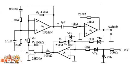
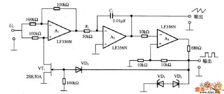
Low-distortion two-phase oscillator circuit diagram
Published:2012/11/9 20:23:00 Author:Ecco | Keyword: Low-distortion, two-phase oscillator
In the circuit, A1 is used as inverting amplifier, the input-output phase difference is 180°, the integrators A2 and A3 have 90 ° phase shift, therefore, the entire circuit has a phase lag of 360 °, if the loop gain is greater than 1, the circuit will generate oscillation. In order to get the oscillation stability, the R5 and VT1 leakage - source equivalent resistors are connected in series.
(View)
View full Circuit Diagram | Comments | Reading(1709)
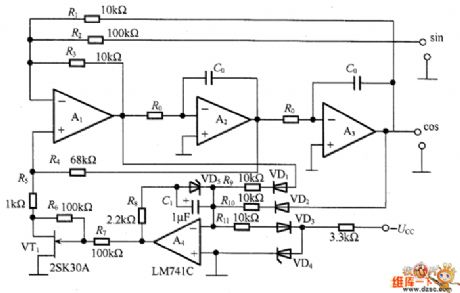
Simple two-phase oscillator circuit diagram
Published:2012/11/9 20:33:00 Author:Ecco | Keyword: two-phase oscillator
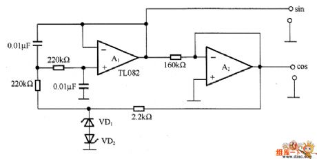
In order to get sine and cosine waves, the circuit is oscillation stabilization circuit without automatic gain control loop, and it can get a stable oscillation output when it is in low frequency. This two-phase oscillator is commonly used as the AC motor signal generator, and it can also be used for the rectangular coordinate transform source or graphic display on the X-Y monitor. In the circuit, A1 constitutex a low pass filter circuit, A2 is an integrator.
(View)
View full Circuit Diagram | Comments | Reading(1542)
The oscillator and trigger circuit with operational amplifier
Published:2012/10/29 21:34:00 Author:Ecco | Keyword: oscillator , trigger , operational amplifier
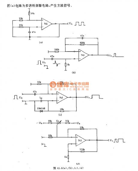
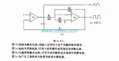
Fig a shows a multivibrator circuit which can generate square wave signal; Figure b is a flip-flop circuit which uses the under edge of the input signal to generate a trigger pulse signal. Figure c is a monostable circuit which can be used for waveform shaping or other signal conversion circuits. Figure d shows a Schmitt trigger circuit for waveform shaping or other signal conversion circuit. Figure e is a triangle wave and square-wave signal generator circuit.
(View)
View full Circuit Diagram | Comments | Reading(2114)
Commonly used simple oscillator circuit diagram
Published:2012/10/17 22:16:00 Author:Ecco | Keyword: oscillator
Figure (a) is the square wave output circuit, in the circuit, the op amp A1 is added a positive feedback, i.e., feedback resistor R2 is connected between the noninverting input and output terminals to form a comparator circuit with the delay characteristics. The voltage on R1 and the charging and discharging voltageof capacitor C1 cause oscillation from comparison. High and low level time of output square wave can be set independently, and the oscillation frequency is determined by the high and low level time, namely, it uses diodes VD1 and VD2, potentiometer RP1 and RP2 to set the charging and discharging time of capacitor C1.
(View)
View full Circuit Diagram | Comments | Reading(1424)
Linear voltage-controlled oscillator circuit diagram
Published:2012/10/17 22:05:00 Author:Ecco | Keyword: Linear, voltage-controlled oscillator
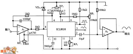
It uses ICL8038 to form a linear voltage controlled oscillator with output frequency and input voltage being proportional. In the circuit, A1 is used to improve C1 charging and discharging constant current circuit characteristics, so that the output frequency and relative input voltage have a linear relationship, A2 is the sine wave output buffer. RP1 is used to adjust the offset voltage, RP2 is used to adjust the high-frequency symmetry, RP3 is used to adjust the low-frequency symmetry, RP3 and RP4 are used to adjust the sine-wave distortion degree.
(View)
View full Circuit Diagram | Comments | Reading(2417)
Voltage - controlled oscillator circuit diagram with operational amplifier
Published:2012/10/17 23:03:00 Author:Ecco | Keyword: Voltage - controlled oscillator , operational amplifier
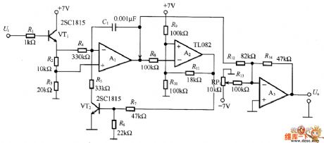
The circuit uses integrator A1 and delay comparator A2 to form a triangular wave oscillator, but the circuit is not directly integrating the output of A2, but it's controlled for integrating, therefore, the obtained oscillation frequency and control voltage are proportional, i.e. the so-called voltage-controlled oscillator. In the circuit, when VT2 gets conduction, the discharging slope rate of C1 is contrary to charging to generate a triangular wave. Saturation voltage of the op amp A2 affects Delay comparator threshold. Thus, the circuit is not suitable for high accuracy circuit. A3 is level-shifting circuit.
(View)
View full Circuit Diagram | Comments | Reading(2953)
Basic JFET Pierce Crystal Oscillator
Published:2012/9/17 21:42:00 Author:Ecco | Keyword: Basic , JFET, Pierce , Crystal Oscillator
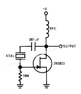
This circuit is a series of JFET Pierce Crystal Oscillator. JFET Pierce crystal oscillator allows a wide range of crystal frequencies to be used without modification of the circuit. Since the JFET gate did not contain crystals, Q both maintained that insure a good frequency stability. (View)
View full Circuit Diagram | Comments | Reading(3660)
Simple Wien-Bridge Oscillator
Published:2012/9/17 21:40:00 Author:Ecco | Keyword: Simple, Wien-Bridge Oscillator
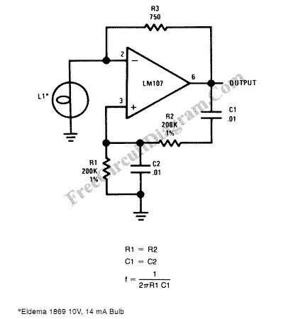
Incandescent lamp has been used to reduce harmonic distortion in sine oscillator circuit. The nonlinear resistance characteristic of the lamp filament help the circuit to shape the signal to approximate the ideal sine wave. Here is the classic Wien-bridge oscillator circuit using the incandescent lamp.
Source: freecircuitdiagram (View)
View full Circuit Diagram | Comments | Reading(0)
| Pages:5/54 1234567891011121314151617181920Under 20 |
Circuit Categories
power supply circuit
Amplifier Circuit
Basic Circuit
LED and Light Circuit
Sensor Circuit
Signal Processing
Electrical Equipment Circuit
Control Circuit
Remote Control Circuit
A/D-D/A Converter Circuit
Audio Circuit
Measuring and Test Circuit
Communication Circuit
Computer-Related Circuit
555 Circuit
Automotive Circuit
Repairing Circuit