
Filter Circuit
Index 18
FOURTH_ORDER_LOW_PASS_BUTTERWORTH_FILTER
Published:2009/6/16 2:27:00 Author:May
View full Circuit Diagram | Comments | Reading(912)
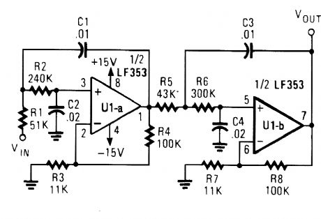
BANDPASS_FILTER
Published:2009/6/16 2:26:00 Author:May
View full Circuit Diagram | Comments | Reading(111)
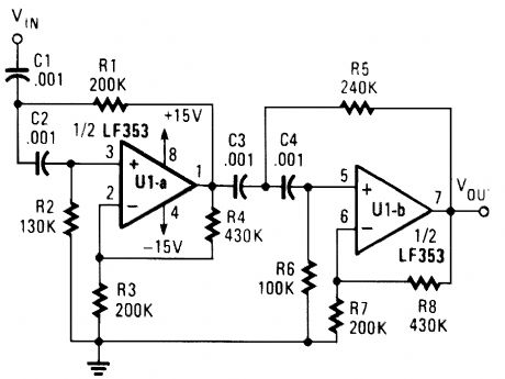
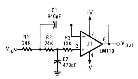
HIGH_Q_BANDPASS_FILTER
Published:2009/6/16 2:24:00 Author:May
View full Circuit Diagram | Comments | Reading(1920)
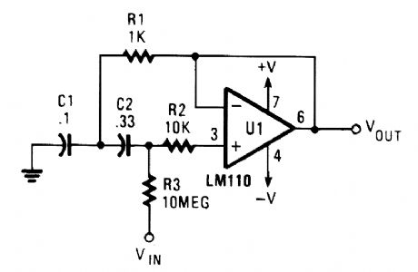
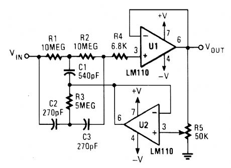
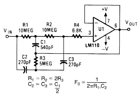
TUNABLE_NOTCH_FILTER
Published:2009/6/16 2:23:00 Author:May
View full Circuit Diagram | Comments | Reading(1190)
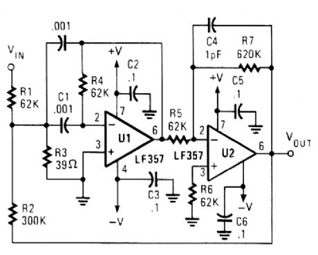
FOURTH_ORDER_HIGH_PASS_BUTTERWORTH_FILTER
Published:2009/6/16 2:22:00 Author:May
View full Circuit Diagram | Comments | Reading(968)
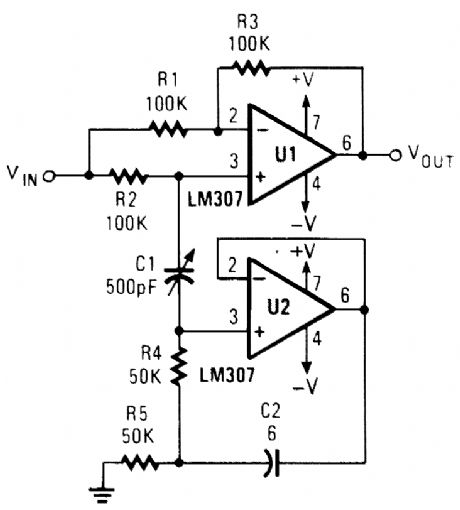
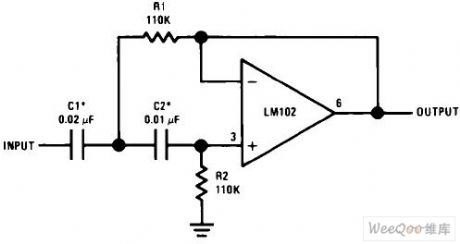
ADJUSTABLE_Q_NOTCH_FILTER
Published:2009/6/16 2:21:00 Author:May
View full Circuit Diagram | Comments | Reading(2)
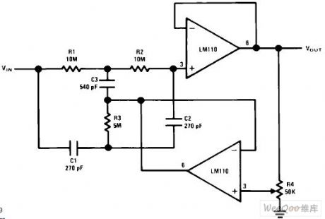
UNIVERSAL_STALE_VARIABLE_FILTER
Published:2009/6/16 2:19:00 Author:May
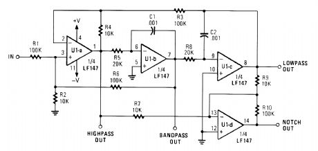
View full Circuit Diagram | Comments | Reading(660)
HIGH_Q_NOTCH_FILTER
Published:2009/6/16 2:18:00 Author:May
View full Circuit Diagram | Comments | Reading(1)
ACTIVE_LOW_PASS_FILTER
Published:2009/6/16 2:18:00 Author:May
View full Circuit Diagram | Comments | Reading(807)
Low pass active filter circuit
Published:2011/7/20 0:43:00 Author:Fiona | Keyword: Low pass, active filter

Low pass active filter circuit is shown as above:
(View)
View full Circuit Diagram | Comments | Reading(779)
High pass active filter circuit
Published:2011/7/20 0:43:00 Author:Fiona | Keyword: High pass, active filter
High pass active filter circuit is shown as above:
(View)
View full Circuit Diagram | Comments | Reading(908)
Q adjustable notching filter circuit
Published:2011/7/17 2:03:00 Author:Fiona | Keyword: notching filter
Q adjustable notching filter circuit is shown as above:
(View)
View full Circuit Diagram | Comments | Reading(824)
Humidity measurement circuit with temperature compensation
Published:2011/7/1 5:47:00 Author:Fiona | Keyword: Humidity measurement, temperature compensation
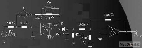
In the actual application,it needs to consider linear processing and temperature compensationfor humidity sensor,and often uses operation amplifier to constitute humidity measurement circuit.The figure is the humidity measurement circuit.Rt is thermosensitive resistor (20kΩ, B = 4100K); RH is the H204C humidity sensor,operational amplifier type is LM2904.Humidity voltage characteristics and temperature characteristic of the circuit demonstrate that: in (30% ~ 90%) RH, 15 ℃ ~ 35 ℃ range,the humidity errorexpressed bythe output voltage is less than 3% RH. (View)
View full Circuit Diagram | Comments | Reading(1404)
Shared RF and base oscillator
Published:2011/7/10 23:16:00 Author:leo | Keyword: Shared RF, shared base
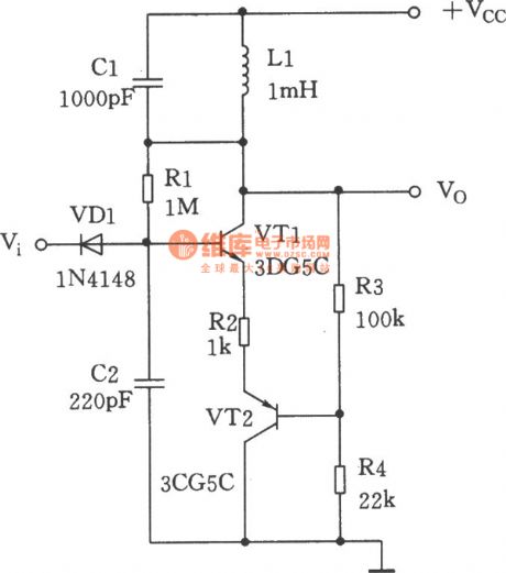
The picture shows a simple oscillator with high stability. It can start automatically with the work voltage of 12 V and work current of 1mA. Its drive circuit is D type amplifier with low output resistance and high output amplitude. Its work voltage coverage is from 2 V to 24 V and it also has other excellent features. Oscillator frequency is decided by LI and CI. As the picture shows, when the frequency of the selected component is 160kHz, time constant RI and CI will be longer than oscillating period. (View)
View full Circuit Diagram | Comments | Reading(995)
TEX888H Communication Monolithic Micro-Computer Integrated Circuit Diagram
Published:2011/7/10 6:15:00 Author:Vicky | Keyword: Communication , Monolithic , Micro-Computer
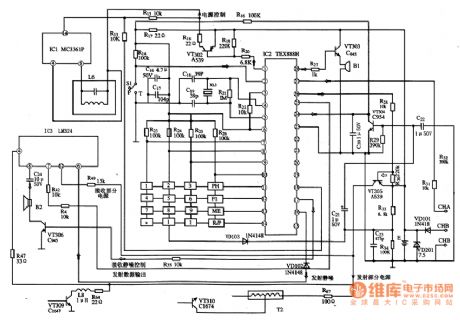
TEX888H is a communication monolithic micro-computer integrated circuit. It is usually used as mobile phone control circuit in cordless telephone.
Typical applied circuit diagram of mobile phone control which is composed of IC TEX888H is shown in picture 1.
Note: When dialing the number, failure in dialing is easy to happen to the mobile. Under such circumstance, check whether the keys are short-circuits or not first, whether the conductive rubber resistance becomes larger or not, and whether the inside mobile is affected with damp or not.
If password failure happens, you might emphasis on the check of the 18 pin of TEX888H and other exterior components. The possible reason of the malfunction can be judged by testing the dynamic or quiescent voltage of the pin. (View)
View full Circuit Diagram | Comments | Reading(3137)
TMP47C400RN Microwave/Oven Monolithic Micro Computer Control Integrated Circuit Diagram
Published:2011/7/3 1:56:00 Author:Vicky | Keyword: Microwave, Oven , Monolithic Micro Computer Control
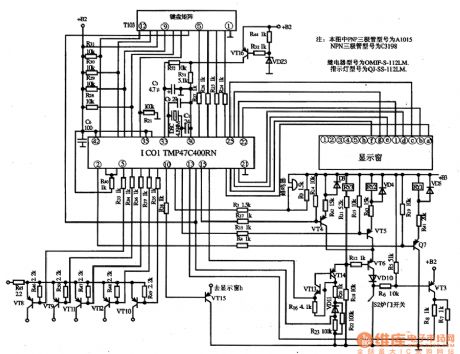
Picture 1 is the typical applied circuit diagram of TMP47C4OORN integrated circuit.
TMP47C400RN is a chip specially designed by Japanese Toshiba Corporation for microwave/oven.
1 functions and features
TMP47C400RN integrated circuit includes keyboard matrix circuit, clock oscillator circuit, motion circuit, reset circuit, microwave control circuit, oven light control circuit and other accessory circuits.
2 pin functions and datum
TMP47C400RN integrated circuit adopts 42 pins in biserial package.
3 typical applied picture
Typical applied circuit of IC TMP47C400RN is shown in the above picture.
Note: When the microwave or oven does not work, you should first check if the 12V AC in the pin 42 of the IC TMP47C4OORN is normal or not, then check the reset signal in the pin 33 (it presents low level at the moment of starting up, and high level during normal work) and the clock oscillating signal pins 31&32.
(View)
View full Circuit Diagram | Comments | Reading(5162)
the sawtooth-wave circuit of complementary tube
Published:2011/6/30 6:11:00 Author:Fiona | Keyword: sawtooth-wave, complementary tube
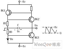
The picture shows the sawtooth-wave circuit of complementary tube.This is self-oscillating complementary sawtooth-wave circuit which the switching device is composed of BG1,BG2 and controls the timing capacitor C to charge and discharge,BG3 is constant flow pipe.When BG1, BG2 are closed, the constant current Ic3 charges to C(polarity is shown as the picture) the output voltage uo decreases with linear time, this is a scanning voltage positive process, when the capacitor voltage Uc drops to the BG2 conduction valve voltage, BG2 starts to conduct,BG1,BG2 arrive at the saturated state after a positive feedback chain reaction,at this time, when you reach a saturation point C remains at saturation without returning to the OFF state through BG1, BG2.
(View)
View full Circuit Diagram | Comments | Reading(721)
complementary tube monostable circuit
Published:2011/6/30 6:35:00 Author:Fiona | Keyword: complementary tube, monostable
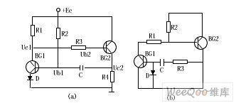
Picture shows the two forms of complementary tube monostable circuit, Figure (b) is complementary tube monostable circuit which the two tubes keep saturation in ordinary state. When it meets conditions,R2 <β1,R1 and R3 <β2, R4,the circuit is in two tubes steady states,when the negative pulse is used at the base BG1, BG1 is out of saturation, and causes a reaction Uc1 ↑ → Ub2 ↑ → Uc2 ↓ → Ub1 ↓.The result of a positive feedback chain reaction is that BG1, BG2 are closed, this is the temporary steady state.At this point C discharges to power supply through R2, R4,it enters two tube saturated stable state after discharging.Diode D is to prevent voltage of C puncturing BG1's base - emitter junction, the pulse width is:
tr=0.7(R2+R4)C
(View)
View full Circuit Diagram | Comments | Reading(1108)
Block Circuit Diagram of Internal LM567CN Integrated Circuit
Published:2011/6/15 8:20:00 Author:Vicky | Keyword: Block Circuit Diagram
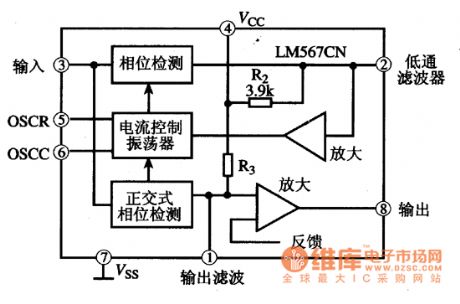
LM567CN is a PLL audio coding integrated circuit. A high-powered cordless phone often uses two pieces of this circuit, taking charge of identifying pilot frequency signal when mobile is off hook and calling signal of the mobile to host machine respectively. (View)
View full Circuit Diagram | Comments | Reading(1169)
Typical Applied Circuit Diagram of LM567CN Integrated Circuit
Published:2011/6/15 8:19:00 Author:Vicky | Keyword: Typical Applied Circuit Diagram
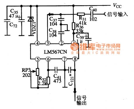
Typical Applied Circuit
Typical applied circuit of decoding circuit, which is composed of LM567CN Integrated Circuit, is shown in the following picture.
(View)
View full Circuit Diagram | Comments | Reading(3380)
| Pages:18/21 1234567891011121314151617181920Under 20 |
Circuit Categories
power supply circuit
Amplifier Circuit
Basic Circuit
LED and Light Circuit
Sensor Circuit
Signal Processing
Electrical Equipment Circuit
Control Circuit
Remote Control Circuit
A/D-D/A Converter Circuit
Audio Circuit
Measuring and Test Circuit
Communication Circuit
Computer-Related Circuit
555 Circuit
Automotive Circuit
Repairing Circuit