
Filter Circuit
Index 6
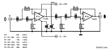
300_TO_3400Hz_SECOND_ORDER_SPEECH_FILTER
Published:2009/7/9 0:03:00 Author:May

Using two op amps,this filter is designed for second-order response.It has a bandpass of 300 to 3 400Hz,for applications In speech or telephone work. (View)
View full Circuit Diagram | Comments | Reading(2327)
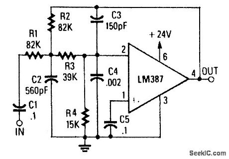
TWO_SECTION_300_3000Hz_SPEECH_FILTER
Published:2009/7/9 0:01:00 Author:May
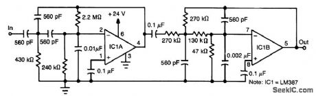
An LM387 dual low-noise amplifier is used in an active filter. Both sections are used to produce second-order HP and LP filters, respectively. (View)
View full Circuit Diagram | Comments | Reading(1736)
ANTIALASING_AND_SYNC_COMPENSATION_FILTER
Published:2009/7/8 23:58:00 Author:May
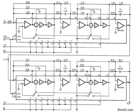
Two dual-biquad filter ciUps and some external components form a multipurpose filter to reconstruct D/A converter signals. Connected to a converter’s output, the filter provides antialiasing, reduces the D/A converter’s quantization noise, and compensates for sin(πx) ÷ (πx)-the sync function (attenuation).
The circuit incorporates an inverse-sync function that operates to one-third of the converter’s sample rate. Beyond one-third, the filter’s response shifts to a stopband filter, which provides -70 dB attenua-tion. This attenuation conforms to the converter’s inherent signal-to-noise ratio and quantization error.
To prevent aliasing, the stopband edge must be no higher than the Nyquist frequency (fsn÷2). To achieve 70-dB stopband rejection with this eighth-order filter requires a transition ratio (fSTOPgAND÷fPASSsAND) of 1.5, which sets the passband’s upper limit at fS÷3.
Notice also that you can apply a simple divide-by-64 circuit to the 192-kHz clock frequency to set the necessary 3× ratio between the converter’s sample rate and the filter’s 1-kHz comer frequency. The V+, V-, and the FO through F5 connections program each filter chip for an fCLK/f0 ratio of 191.64. (View)
View full Circuit Diagram | Comments | Reading(931)
LOW_COST_CRYSTAL_FILTERS
Published:2009/7/8 23:35:00 Author:May
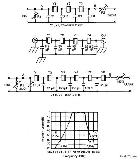
Low-cost CB crystals can be used for these 9-MHz crystal ladder filters. Notice that the 27-MHz crystals (3rd overtone) are used on their fundamental frequencies. (View)
View full Circuit Diagram | Comments | Reading(2542)
TUNABLE_BANDPASS_FILTER
Published:2009/7/8 23:33:00 Author:May
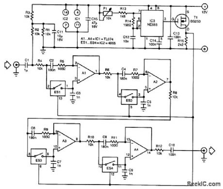
One of the difficulties in the design of higher-order tunable bandpass filters is achieving correct track-ing of the variable resistors in the RC networks. The use of switched capacitor networks can obviate that difficulty, as is shown in this filter.
The filter can be divided roughly into two stages: an oscillator that controls the electronic switches and the four phase-shift networks that provide the filtering proper. The oscillator, based on a 555, generates a pulsating signal whose frequency is adjustable over a wide range: the duty factor varies from 1:10 to 100:1.
Electronic switches ES1 through ES4 form the variable resistors whose value is dependent on the frequency of the digital signal. The operation of these switches is fairly simple. When they are closed, their resistance is about 60Ω; when they are open, it is virtually infinitely high. If a switch is closed for, say, 25% of the time, its average resistance is therefore 240Ω. Varying the open:closed ratio of each switch varies the equivalent average resistance. The switching rate of the switches must be much greater than the highest audio frequency to prevent audible interference between the audio and the clock signals.
The input signal causes a given direct voltage across C1, so the op amp can be operated in a quasisym-metric manner, in spite of the single supply voltage. The direct voltage is removed from the output signal by capacitor C10.
The fourth-order filter in the diagram can be used over the entire audio range and it has an ampliftca-tion of about 40, although this depends to some extent on the clock frequency. The bandwidth depends mainly on the set frequency. The circuit draws a current of not more than 15 mA. (View)
View full Circuit Diagram | Comments | Reading(4741)
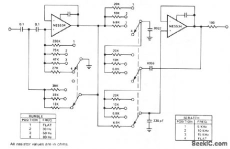
TURNTABLE_RUMBLE_FILTER
Published:2009/7/8 23:27:00 Author:May
Many record players unfortunately exhibit two undesired side effects: rumble (noise caused by the motor and the turntable) and other low-frequency spurious signals. The active high-pass Chebyshev filter presented here was designed to suppress those noises. The filter has a 0.1-dB ripple characteristic and a cut-off point of 18 Hz.
The choice of a Chebyshev filter might not seem optimum for audio purposes, but because of its 0.1-dB ripple in the pass band it behaves very much like a Butterworth type. Its advantage is that the response has steeper skirts (which are calculated curves). Frequencies below 10 Hz are attenuated by more than 35 dB. The phase behavior in the pass band shows a gradual shift so that its effect on the repro-duced sound is inaudible.
If the filter is used in a stereo installation, the characteristics of both filters must be identical or nearly so. Phase differences between channels can be heard-perhaps not so much at lower frequencies, but certainly in the midranges. To ensure identity and also to obtain the desired characteristics, capacitors C1 through C5 must be selected carefully. It does not matter much whether their value is 467 or 473 pF; this difference only causes a slight shift of the cut-off point. However, they must be identical within that 1% tolerance. For symmetry of channels, the capacitors can be paired and then used in either channel at the corresponding position.
The diagram shows theoretical values for the resistors: their practical values are given in the table.The prototype was constructed with 5% metal-film types from the E12 series and these were used with-out sorting. Their tolerance was perfectly acceptable in practice.
The current drawn by the circuit is purely that through the op amp and it amounts to about 4 mA. The high cut-off point is also determined by the op amp and it lies at about 3 MHz.
The only problem that cannot be foreseen is a possible coupling capacitor in the signal source. That component will be in series with C1 and this might adversely affect the frequency response. However, if its value is greater than 47 μF, it will have little if any effect; if it is below that value, it is best removed; C1 will assume its function. (View)
View full Circuit Diagram | Comments | Reading(2897)
SCRATCH_FILTER
Published:2009/7/9 1:34:00 Author:May
Designed to produce 12-dB/octave roll-off above the 10-kHz cutofffrequency, this LP active filter will help reduce needle scratch on records. It uses an LM387low-noise amplifier IC. (View)
View full Circuit Diagram | Comments | Reading(0)
SECOND_ORDER_100_Hz_HIGH_PASS_FILTER
Published:2009/7/9 1:32:00 Author:May
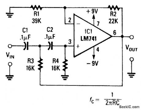
This second-order filter can be scaled change the cutoff frequencies. (View)
View full Circuit Diagram | Comments | Reading(953)
TUNABLE_AUDIO_FILTER
Published:2009/7/8 22:54:00 Author:May
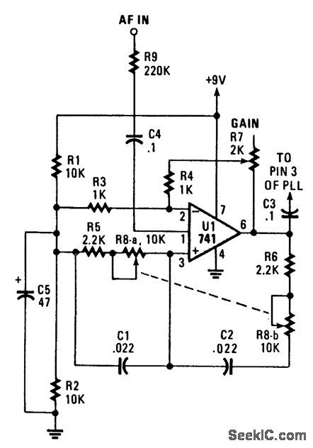
This circuit uses a Wien Bridge and variable negative feedback. R7 controls the gain and R8A and R8B controls the tuned frequency. (View)
View full Circuit Diagram | Comments | Reading(0)
FAST_RESPONSESETTLINGLOW_PASS_FILTER
Published:2009/7/8 22:44:00 Author:May
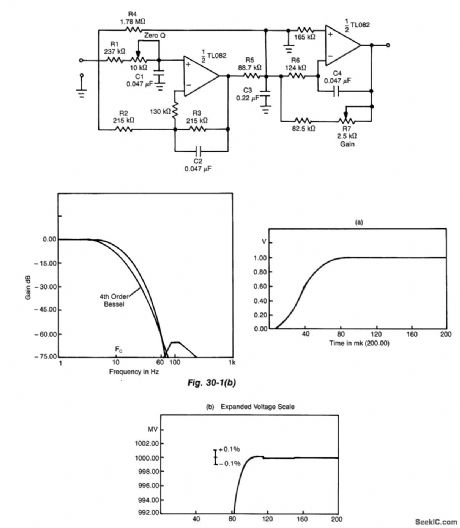
This circuit uses a Wien Bridge and variable negative feedback. R7 controls the gain and R8A and R8B controls the tuned frequency. (View)
View full Circuit Diagram | Comments | Reading(765)
TWIN_T_NOITCH_FILTER
Published:2009/7/8 22:09:00 Author:May
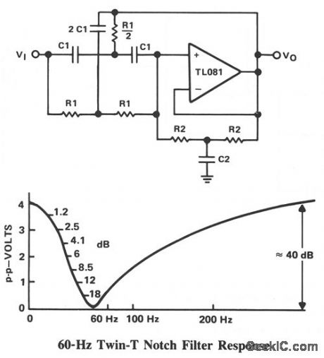
This filter is used to reject or block a frequency or band of frequencies. These filters are often designed into audio and instrumentation systems to eliminate a single frequency, such as 60 Hz. Commercial grade components with 5%-1070 tolerance produce a null depth of at least 30 to 40 dB. When a twin-T network is combined with a TL081 op amp in a circuit, an active filter can be implemented. The added resistor capacitor network, R2 and C2, work effectively in parallel with the original twin-T network, on the input of the filter. These networks set the Q of the filter. The op amp is basically connected as a unity-gain voltage follower. The Q is found from:
R2 C1 Q = — = — 1R2 C2For a 60-Hz notch filter with a @ of 5, it is usually best to pick the C1 capacitor value and calculate the resistor R1. Let C1 = 0.22 μF. Then:
R1 = 12 KΩ R1 = 120 KΩ C2 = 0.047/μF
Standard 5% resistors and 10% capacitors produce a notch depth of about 40 dB, as shown in the frequency response curve.
(View)
View full Circuit Diagram | Comments | Reading(1081)
DIODE_SWITCHED_IF_FILTER
Published:2009/7/8 5:06:00 Author:May
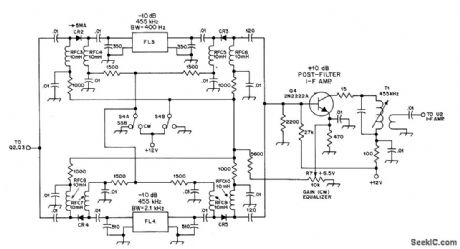
Used in 1.8-2 MHz communication receiver having wide dynamic range 1N914 diodes select collins mechanical filter F455FD-04 FL3 (400-Hz bandwidth) or F455FD-25 FL4(2.5-kHz bandw)Reverse biasis applied to nonconducting diodes to lesson leakage through switching diodes Filteris located between IF preamρ and main IF strip of receiver Two-part article gives all other circuits of receiver,-D.DeMaw,His Eminence-the Receiver,QST,Part 1-June 1976,p 27-30(Part2-July 1976,p 14-17). (View)
View full Circuit Diagram | Comments | Reading(886)
RUMBLE_SCRATCH_FILTER
Published:2009/7/8 3:26:00 Author:May
This is a variable bandpass amplifier with adjustable low- and high-frequency cutoffs. (View)
View full Circuit Diagram | Comments | Reading(0)
WIEN_BRIDGE_FILTER
Published:2009/7/8 3:24:00 Author:May
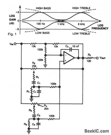

Most audio tone controls affect midband gain, and they often create booming or hissing sounds when activated. You can avoid these problems by using a dual Wien-bridge filter to provide independent control of the treble and bass frequencies.Experiments with equalizers indicate that the optimum center frequencies are about 100 Hz and 8 kHz. Using the relationf = (2πRC)-1, set the Fig. 1 values accordingly:
100 Hz: R1 = 15 KΩ; C1 = 0.1 μF 8 kHz: R2 = 16 KΩ; C2 = 1.3 μFR3 and C3 provide stability. You obtain a ± 9 dB variation of treble and bass by adjusting potentiometers R4 and R5, respectively. The filter's frequency response is shown in Fig. 2. (View)
View full Circuit Diagram | Comments | Reading(1781)
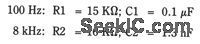
COIN_FLIPPER
Published:2009/7/7 21:47:00 Author:May
One of LEDs comes on when S1 is pressed, to simulate tossing of coin. LEDs can be labeled HEADS and TAILS if desired. Transistor types are not critical. For true random results, voltage between collectors of transistors should be 0 V with S2 closed and S1 open.-Circuits, 73 Magazine, June 1975, p 161. (View)
View full Circuit Diagram | Comments | Reading(0)
1_kHz_N_PATH_NOTCH_FILTER
Published:2009/7/7 21:24:00 Author:May
Combination of DG508 eight-channel CMOS multiplexer with low-pass and bandpass active filters provides 1-kHZ notch filter having Q of 1330 and 3-dB bandwidth of 0.75 Hz at 1 kHz. Low-pass filter introduces 180° phase shift at 1 kHz. Amplifier sums original signal in phase-shifted bandpass output from N-path filter, canceling 1-kHz components in original signal to produce desired notch characteristic.-″Analog Switches and Their Applications, SiIiconix. Santa Clara,GA,1976,p5-18-5-20. (View)
View full Circuit Diagram | Comments | Reading(2310)
HEADS_TAILS_FLIPPER
Published:2009/7/7 21:18:00 Author:May
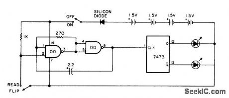
Uses only half of 7400 quad NAND gate as gated clock driving half of 7473 JK flip-flop. With power switch closed, LEDs representing heads and tails flash on and off at clock frequency, Closing FLIP switch stops clock randomly, leaving one LED on to give equivalent of tossing coin for heads/tails call.-G. Young,JK Flip-Flops and Clocked Logic, Kilobaud, July 1977, p 66-70 and 72-73. (View)
View full Circuit Diagram | Comments | Reading(1348)
COMMUTATING_BANDPASS_FILTER
Published:2009/7/7 20:04:00 Author:May
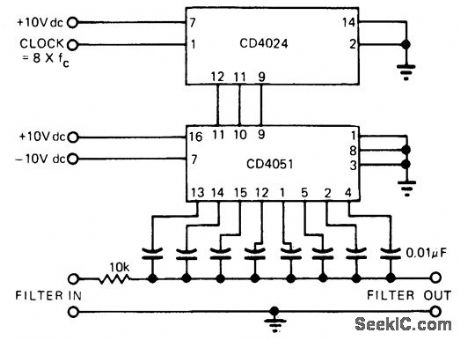
CD4051 analog multiplexer serves for commutation and switching of eight low-pass filter sections. Multiplexer is driven by CD4024 binary counter that is clocked at 8 times desired 100-kHz center frequency Can be tuned by varying commutating frequency.J Tracy, CMOS Offers New Aρproach to Commutating Filters. EDN Magazine, Feb,5,1974.ρ94-95.
(View)
View full Circuit Diagram | Comments | Reading(4417)
1_kHz_COMB_FILTER
Published:2009/7/7 19:58:00 Author:May
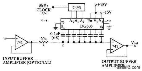
DG508 eight-channel CMOS multiplexer is used in comb filter having fundamental frequency of 1 kHz. Sampling action provides response at each harmonic multiple except at 8 and 16 kHz (no response at Nf0 or 2Nf0). Used in selective filtering of periodic signals from background of nonperiodic noise interference, 7493 TTL binary counter provides necessary 3-bit binary count sequence from 8-kHz clock. Q is 50.- Analog Switches and Their Applications, Siliconix, Santa Clara, CA, 1976, p 5-17-5-18. (View)
View full Circuit Diagram | Comments | Reading(2084)
COIN_FLIPPER
Published:2009/7/7 6:56:00 Author:May
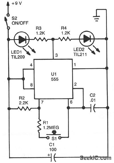
The circuit is basically a 555 astable circuit that divides two LEDs, LED1 and LED2. LED2 is switched on when the output of U1 is high, and LED1 is activated when its output is low. When U1 oscillates, LED1 and LED2 switch on alternately as the output of U1 switches from state to state. Resistor R1's value is high in comparison to R2, so the waveform at the output is a square wave with a mark/space ratio of nearly one-to-one. When you release S1, you break the circuit and U1 latches whatever the output state happens to be at the time. (View)
View full Circuit Diagram | Comments | Reading(1505)
| Pages:6/21 1234567891011121314151617181920Under 20 |
Circuit Categories
power supply circuit
Amplifier Circuit
Basic Circuit
LED and Light Circuit
Sensor Circuit
Signal Processing
Electrical Equipment Circuit
Control Circuit
Remote Control Circuit
A/D-D/A Converter Circuit
Audio Circuit
Measuring and Test Circuit
Communication Circuit
Computer-Related Circuit
555 Circuit
Automotive Circuit
Repairing Circuit