
Filter Circuit
Index 8
RUMBLE_SCRATCH_FILTER
Published:2009/7/6 1:24:00 Author:May
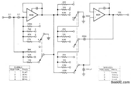
Used after pre-amp in high-quality audio system to improve reproduction of phonograph records. Two-pole Butterworth design has switchable breakpoints providing any desired degree of filtering.- Signetics Analog Data Manual, Signetics, Sunnyvale, CA, 1977, p 638-639. (View)
View full Circuit Diagram | Comments | Reading(2119)
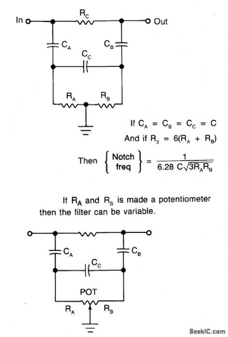
PASSIVE_BRIDGED,DIFFERENTIATOR_TUNABLE_NOTCH_FILTER
Published:2009/7/5 22:14:00 Author:May
View full Circuit Diagram | Comments | Reading(1213)
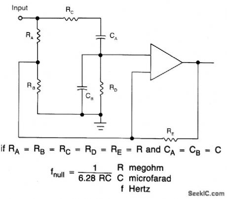
WIEN_BRIDGE_NOTCH_FILTER
Published:2009/7/5 22:12:00 Author:May
View full Circuit Diagram | Comments | Reading(974)
ACTIVE_BAND_REJECT_FILTER
Published:2009/7/5 22:12:00 Author:May
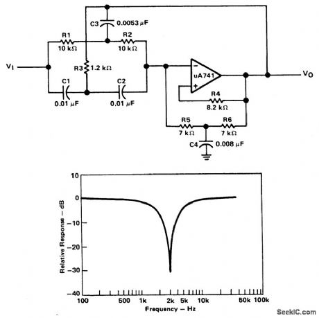
A filter with a band-reject characteristic is frequently referred to as a notch filter.A typical circuit using a μA741 is the unity-gain configuration for this type of active filter shown. The filter response curve shown is a second-order band-reject filter with a notch frequency of 3 kHz. The resulting Q of this filter is about 23, with a notch depth of -31 dB. Although three passive T networks are used in this application, the operational amplifier has become a sharply tuned low-frequency filter without the use of inductors or large-value capacitors. (View)
View full Circuit Diagram | Comments | Reading(4795)
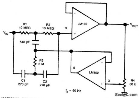
AUDIO_NOTCH_FILTER
Published:2009/7/5 22:10:00 Author:May

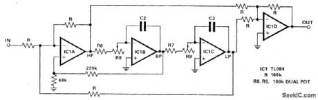
With the circuit shown here the response at one octave off tune is within 10% of the far out response: notch sharpness may be increased or reduced by reducing or increasing respectively the 68 K ohm resistor. Linearity tracking of R8 and R9 has no effect on notch depth. The signals at HP and LP are always in antiphase, notch will always be very deep at the tuned frequency, despite tolerance variations in R6-9 and C2, C3. (View)
View full Circuit Diagram | Comments | Reading(1160)
TUNABLE_AUDIO_NOTCH_FILTER_CIRCUIT
Published:2009/7/5 22:09:00 Author:May
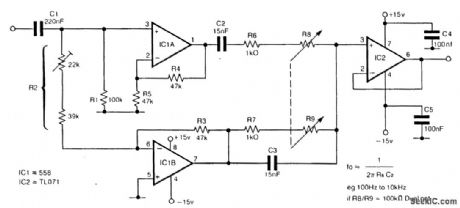
The circuit requires only one dual-ganged potentiometer to tune over a wide range ; if necessary over the entire audio range in one sweep. The principle used is that of the Wien bridge, fed from anti-phase inputs. The output should be buffered as shown with a FET input op amp, particularly if a high value pot is used. An op amp with differential outputs (eg., MC1445) may be used in place of the driver ICS; R2 may be made trimmable to optimize the notch. (View)
View full Circuit Diagram | Comments | Reading(2302)
550_Hz_NOTCH_FILTER
Published:2009/7/5 22:08:00 Author:May
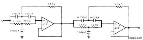
The circuit produces at least 60 dB of attenuation。f the notch frequency. (View)
View full Circuit Diagram | Comments | Reading(978)
1800_Hz_NOTCH_FILTER
Published:2009/7/5 22:07:00 Author:May
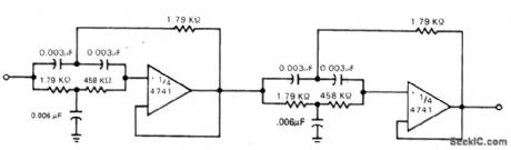
The circuit produces at least 60 dB of attenuation of the notch frequency. (View)
View full Circuit Diagram | Comments | Reading(842)
ADJUSTABLE_Q_NOTCH_FILTER
Published:2009/7/5 22:07:00 Author:May
In applications where the rejected signal might deviate slightly from the null on the notch network, it is advantageous to lower the Q of the network. This insures some rejection over a wider range of input frequencies. The figure shows a circuit where the Q may be varied from 0.3 to 50. A fraction of the output is fed back to R3 and C3 by a second voltage follower, and the notch Q is dependent on the amount of signal fed back. A second follower is necessary to drive the twin T from a low-resistance source so that the notch frequency and depth will not change with the potentiometer setting. (View)
View full Circuit Diagram | Comments | Reading(0)
DOUBLER_FOR_1_Hz_TO_12_MHz
Published:2009/7/5 20:49:00 Author:May
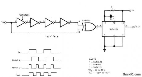
Simple arrangement of EXCLUSIVE-OR,mono,and hex Inverter ICs ρrovides extremely accurate frequency doubling in digital systems, along with waveform symmetry. Article gives design equation Series inverters create about 120 ns of .delay.-V. Rende, Frequency Doubler Operates from 1 Hz to 12 MHz, EDN Magazine, Aug. 20, 1976,p 85. (View)
View full Circuit Diagram | Comments | Reading(2517)
HIGH_SPEED_FIFO
Published:2009/7/5 20:27:00 Author:May
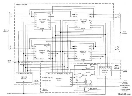
Design is based on Motorola MC10143 register file, with each IC holding 8 words by 2 bits, Circuitincludes write and read enable inputs for cascading two register file packages to memory depth of 16 words. Full master-slave flip-flop operation allows simultaneous read and write. Reset is applied initially to drive both address counters to empty state.To enter data, write clock input is enabled with negative-going pulse. Write addressing is controlled by MC10178 binary counter. Used for stack registers of computing systems when register outputs are read sequentlally in sameorder that data wad entered(first-in first-out).-B.Blood, A High Speed FIFO Memory Usingthe MECL MC10143 Register Fil, Motorola,Phoenix,AZ,1974,AN-730,p 5. (View)
View full Circuit Diagram | Comments | Reading(1690)
DOUBLER_FOR_TACHOMETER
Published:2009/7/5 19:58:00 Author:May
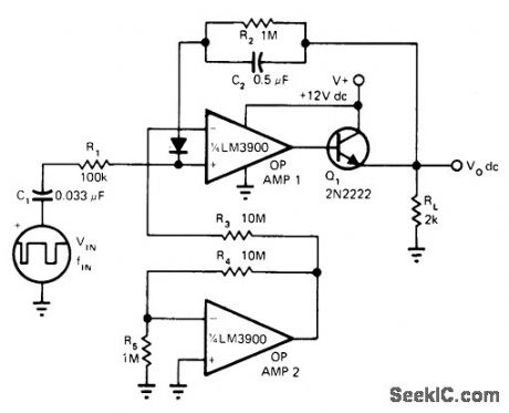
Frequency of input from tachometer is doubled by charging and discharging of C1 to reduce ripplein DC output voltage of tachometer circuit. Opamp 2 provides bias current for opamp 1, while Q1 drives large load currents and provides DC level shift required for bringing output voltage to zero when input frequency is zero.-T. Frederiksen, Frequency-Doubling Tach Operates from a Single Supply,EDN Magazine, June 5, 1977, p 208. (View)
View full Circuit Diagram | Comments | Reading(1620)
SINE_WAVE_DOUBLE_
Published:2009/7/5 19:51:00 Author:May
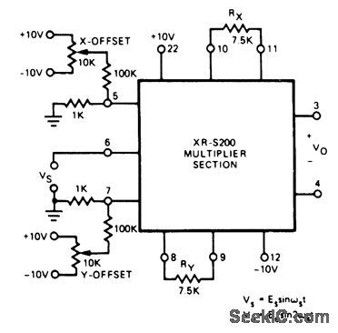
Frequency of sinusoidal input signal VS is doubled to give sine-wave output with total harmonic distortion less than 0.6%,With input of 4 V P-P at 10 kHz、output is1V P-P at 20 kHz. X and Υ offset adjustments are nulled to minimize harmonic content of out-put.-″PhaseˉLocked Loop Data Book,''Exarlntegrated Systems,Sunnyvale,CA,1978,p 9-16. (View)
View full Circuit Diagram | Comments | Reading(847)
FET_DOUBLE
Published:2009/7/5 19:40:00 Author:May
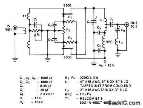
Siliconix E300 matched FETs are connected as common-gateamplifiers in blanced push-push circuit giving up to 100% efficiency as frequency multiplier in UHF range.series-tuned output trap L2C8 increase rejecttion of third-orde harmonics to greater than 70dB.Positive bias of 0.5 V is applied to FET gates to permit inclusion of balance control R2,Gainof doubler is about 1 dB.-''Analog Switches ''and Their Applications,''Siliconix、Santa Clara,CA、1976 p7-52 (View)
View full Circuit Diagram | Comments | Reading(1355)
BROADBAND_LOW_FREQUENCY_DOUBLER
Published:2009/7/4 22:05:00 Author:May
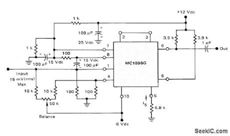
Motorola MC1596G balanced modulator functions as frequency doubler when same signalis injected into both input ρorts (plns 1 and 8),Doubling occurs audio range and up to about 1 MHz.-R.Hejhall,″MC1596 Balanced Modulator,″Motorola,Phoenix、AZ,1975,AN-531,p 10 (View)
View full Circuit Diagram | Comments | Reading(1075)
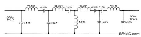
LOW_PASS_PI_SECTION_AF
Published:2009/7/3 5:00:00 Author:May
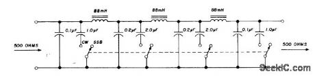
Four-pole doublethrow switch gives choice of 650-Hz cutoff for CW or 2000 Hz for SSB.Filter capacitors are matched Response decreases continuously beyond cutoff frequency,with no loss of attenuation.-E.Noll,Circuits and Techniques,Ham Radio,April 1976,p 40-43. (View)
View full Circuit Diagram | Comments | Reading(894)
80_METER_BANDPASS
Published:2009/7/3 4:59:00 Author:May
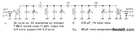
Four-resonator filter for use in 80-meter amateur band has 100-kHz bandwidth, 4.4-dB insertion loss, and 6-60 dB shape factor of 5.16. Filter was designed and aligned at 3.75 MHz; realignment at 3.6 and 3.9 MHz yielded Similar results Artiole covers theory.construction, and adjustment-W Hay-ward,Bandpass Filters for Receiver Preselectors,Ham Radio,Feb,1975,p 18-27. (View)
View full Circuit Diagram | Comments | Reading(927)
SWITCHABLE_AF_FlLTER
Published:2009/7/3 4:58:00 Author:May
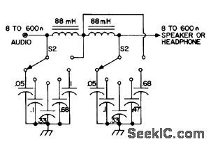
Provides wide range of switch-selected capacitor values for varying cutoff frequencies, to permit use of filter for either phone or CW reception. On CW, circuit improves reception by eliminating higher frequencies that are largely interference.-J. J.Schultz,The Quiet Maker, 73 Magazine, March 1974, p 81-84. (View)
View full Circuit Diagram | Comments | Reading(796)
225_Hz_BANDPASS_RTTY
Published:2009/7/3 4:55:00 Author:May
Used ahead of Limiter in 170-Hz-shift RTTY receiving converter.Chebyshev mesh configuration with 0.1-dB ripple uses inductor to ground for sharpening lower skirt, with capacitive coupling for sharpening upper skirt, to give good symmetry for response curve. Capacitors should be high-Q ty low in frequency. Insertion loss is 6.6 dB and 3-dB bandwidth is 225 Hz, which makes mark and space tones only 1.5 dB down.-A. J. Klappenberger, A High-Performance RTTY Band-Pass Filter, QST, Jan. 1978, p 33. (View)
View full Circuit Diagram | Comments | Reading(681)
1_kHz_FIFTH_ORDER_LOW_PASS
Published:2009/7/3 4:15:00 Author:May
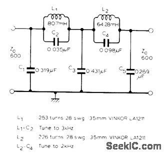
Used with 1-kHz signal generator to remove unwanted harmonics,leaving pure sine wave as required formeasuring distortion in modern audio amplifiefs Attenuation peaks are carefuny positionedto coincide with second and third harmonics,giving 65-dB attenuation of these harmonicsand at least 50-dB attenuation of higher hatmonics.-J A,Hardcastle,1 kHz Source Cleaning Filter,Wireless World,Oct,1978,p 59. (View)
View full Circuit Diagram | Comments | Reading(0)
| Pages:8/21 1234567891011121314151617181920Under 20 |
Circuit Categories
power supply circuit
Amplifier Circuit
Basic Circuit
LED and Light Circuit
Sensor Circuit
Signal Processing
Electrical Equipment Circuit
Control Circuit
Remote Control Circuit
A/D-D/A Converter Circuit
Audio Circuit
Measuring and Test Circuit
Communication Circuit
Computer-Related Circuit
555 Circuit
Automotive Circuit
Repairing Circuit