
Basic Circuit
Index 161
12_V_STROBOSCOPE
Published:2009/7/14 1:37:00 Author:May
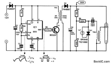
Diode Dl is a polarity-protection device that can be omitted. A 555 is used as an astable with a frequency of about 0.7 kHz. When T1 is on, a current flows through the 6-V winding of TR1. When the collector voltage of T1 is nearly 0, the potential at the anode of D2 must be negative. When T1 becomes reverse-biased, its collector voltage rises to about 12 V and the potential at the anode of D2 must then be positive so that C4 can be charged Never operate the converter without a load. It is, perhaps, advisable to shunt C4 with a 100-kΩ, 1-W resistor. The converter charges C4 to about 300 V. This causes a potential at junction R6-05 of about 100 V. The neon lamp then comes on, so a gate current flows into the thyristor. This comes on and clears the way for C5 to discharge through TR2.This starting transformer produces a secondary voltage of a few thousand volts. This is sufficient for the xenon tube to strike and at the same time discharge C4. Then the operation can start again. The circuit draws a current of about 250 mA, but this depends on the flashing rate and the type of xenon tube. (View)
View full Circuit Diagram | Comments | Reading(1193)
40_METER_CW
Published:2009/7/14 1:37:00 Author:May
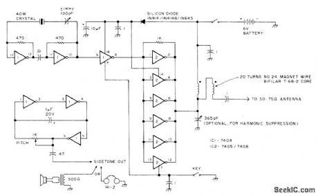
Delivers about 250 mW of RF output, operating from 6-V battery. Sidetone can be monitored with high-impedance headphones or small loudspeaker. Carrier frequency can be tuned up to 1 kHz above and below nominal frequency of 40.meter crystal-Circuits, 73 Magazine, July 1977, p 34.
(View)
View full Circuit Diagram | Comments | Reading(894)
l_KC_SCALER
Published:2009/7/14 1:37:00 Author:May
Glow-tube counter provides driving pulses of about l00 v, using two amplifiers in cascade, both saturated when no signals are present.-H. A. Kampf, Increasing Counting System Reliability, Electronics, 32:37, p 112-113. (View)
View full Circuit Diagram | Comments | Reading(682)
SYNC_FOR_SCR_PARALLEL_INVERTER
Published:2009/7/15 22:40:00 Author:Jessie
Double-output pulse generator uses two relaxation oscillators synchronized by C3 to produce high-energy pulses alternately from two separate sources, in correct timing sequence from instant that supply voltage is switched on. Synchronism is required to prevent inverter failure.-SCR Parallel Inverters in Correct Timing Sequence, Electronic Circuit Design Handbook, Mactier Pub. Corp., N.Y., 1965, p 66. (View)
View full Circuit Diagram | Comments | Reading(1530)
HEADS_OR_TAILS_GAME_CIRCUIT
Published:2009/7/14 1:35:00 Author:May
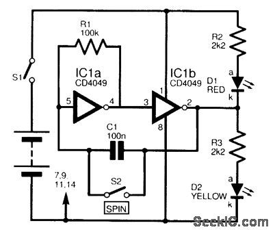
Designed to simulate by electronic means thetossing of a coin,the circuit is based upon a 4049 hex inverter IC, two of which are used. IC1a andIC1b are wired as an astable oscillator, which causes two LEDs(D1 and D2) to alternate rapidly,at a frequency too high to be distinguished by thenaked eye. Both LEDs, therefore, appear to be constantly illuminated. when the SPIN switch S2 is closed, this has the effect of freezing the display,and the LED, which was illuminated at the instantthat the switch was closed, will now be continuously alight. Opening the switch enables the oscillator once more . There is an equal chance of either LED lighting,and the circuit can be used in boardgames, for example, to choose which player will move first. (View)
View full Circuit Diagram | Comments | Reading(970)
WRONG_POLARITY_PROTECTION
Published:2009/7/15 22:38:00 Author:Jessie
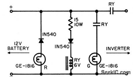
Provides built-in protection of transistors in inverter from incorrect polarity of connection to 12-v battery. Used between inverter and battery. Green bulb G lights and relay operates for correct polarity. With wrong polarity, relay does not operate and red bulb R comes on to indicate error.-J. J. Pirch, Inverter Control, EEE, 11:3, p 44. (View)
View full Circuit Diagram | Comments | Reading(877)
RING_COIJNTER_WITH_VISUAL_READOUT
Published:2009/7/14 1:35:00 Author:May
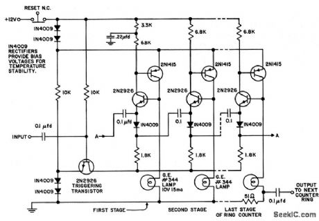
Uses only six components per stage. Combining of counter and indicator functions gives low battery drain. After reset button is re leased, 0.22-mid capacitor insures that first stage turns on. Current is drown by stage only when lamp is on. Any number of stages may be included in ring.- Transistor Manual, Seventh Edition, General Electric Co., 1964, p 203. (View)
View full Circuit Diagram | Comments | Reading(711)
SELF_EXCITED_HALF_BRIDGE
Published:2009/7/15 22:37:00 Author:Jessie
Uses only two transistors. Suitable for both two-phase and three-phase applications. Basic circuits can be connected in series for high-voltage operation. Maximum transistor off voltage equals input voltage of half-bridge, making 80-v inverter practical for germanium transistors and 150 v for silicon.-A. G. Lloyd, Half-Bridge Inverter Provides Economical Three. Phase Power, Electronics, 34137, p 62-65. (View)
View full Circuit Diagram | Comments | Reading(2148)
LOGIC_DRIVES_TRIAC
Published:2009/7/14 1:33:00 Author:May
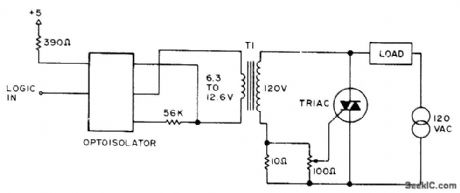
H74C1 optoisolator combined with saturation characteristic of ordinary filament transformer serves to trigger full-wave triac on or off under control of logic input, for energizing AC loads up to rating of triac. Logic 0 (ground level) turns load on, and logic 1 turns it off.-D. D. Mickle, Practical Computer Projects, 73 Magazine, Jan. 1978, p 92-93. (View)
View full Circuit Diagram | Comments | Reading(870)
LOCKOUT_CIRCUIT_
Published:2009/7/14 1:33:00 Author:May
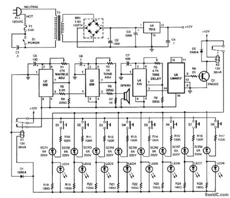
This circuit is used in contests,games,etc When a contestant presses one of the buttons,an SCR triggers,lighting the associated LED and preventing anyone else from actuating the system .U2 and U3 form a warble tone generator, while U4 and U5 provide time delay. (View)
View full Circuit Diagram | Comments | Reading(1984)
POSITIVE_FEEDBACK_BOOSTS_SWITCHING_SPEED
Published:2009/7/15 22:36:00 Author:Jessie
Base resistors R1 and R2 allow addition of cross-coupled positive-feedback capacitors C1 and C2 to increase high-frequency gain of feedback loop and provide energy storage to drive oaf transistor fully on when core saturates.-A. G. Lloyd, Speed-Up Circuits Improve Switching of Transistor Inverters, Electronics, 34:45, p 92-94. (View)
View full Circuit Diagram | Comments | Reading(687)
LOGIC_DRIVES_SCR_
Published:2009/7/14 1:32:00 Author:May
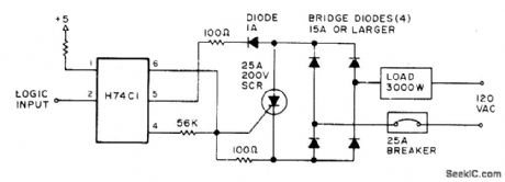
Uses light-activated SCR in H74C1 optoisolator to trigger larger SCR for controlling loads up to 3000 W through bridge diodes, When logic input goes low (to ground), load is energized. Limit for inductive loads is 8 A or about 1000 W if using 25-A SCR.-D. D.Mickle, Practical Computer Projects, 73 Magazine, Jan. 1978, p 92-93. (View)
View full Circuit Diagram | Comments | Reading(1033)
VOICE_EFFECTS_SIMULATOR_CIRCUIT
Published:2009/7/14 1:31:00 Author:May
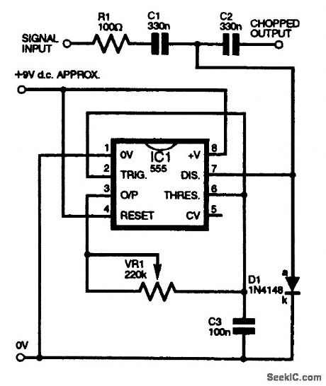
The circuit design shown produces a Dr Who Dalek voice effect by chopping an audio signal at a low frequency. The best frequency seems to be around 50 to 90 Hz, and this is generated by IC1, a 555 timer. The arrangement shown is not an ordinary 555 astable multivibrator, but a hysteresis oscillator, which frees the 555 internal discharge transistor (pin 7) to act as a chopper, shunting the signal to 0 V internally. The chopped frequency is set by VR1, which is adjusted to give the most realistic sound. The input signal should be in the region of 50 to 150 mV rms from a low-impedance source-e.g., possibly a dynamic microphone-to avoid clipping the signal. The diode D1 is optional, and prevents the signal from losing symmetry, if overdriven. The output signal is fed to an external amplifier. The two dc-blocking capacitors C1 and C2 are optional and are needed only if any dc bias is present on the input signal side. (View)
View full Circuit Diagram | Comments | Reading(2563)
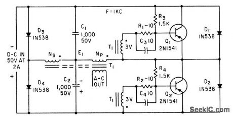
PARALLEL_SQUARE_WAVE_D_C_TO_A_C_INVERTER
Published:2009/7/15 22:33:00 Author:Jessie
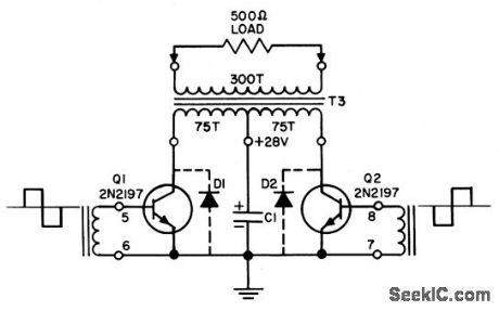
Receives square-wave inputs from separate drive circuit (not shown), causing Q1 to conduct half the time while Q2 is blocking, and vice-versa. Current from 28-v supply flows alternately through halves of transformer primary, to produce 400-cps a-c voltage across load.- Transistor Manual, Seventh Edition, General Electric Co., 1964, p 235. (View)
View full Circuit Diagram | Comments | Reading(722)
450_470_MHz_AT_25_W
Published:2009/7/14 1:27:00 Author:May
Power amplifier for land-mobile 12.5-V transmitter is constructed on double-sided microstrip substrate. Power gain at 470 MHz is 19.5 dB, and overall efficiency is 47%.-G. Young, UHF Microstrip Amplifiers Utilizing G-10 Epoxy-Glass Laminate, Motorola, Phoenix, AZ, 1976,AN-578, p 4. (View)
View full Circuit Diagram | Comments | Reading(615)
CURRENT_ECONOMIZING_DESIGN
Published:2009/7/14 1:26:00 Author:May

Used in 15-stctge counter. Circuit is conventional, but to economize on current, only first three stages operate with relatively high collector currents; for these, RI and R2 +R3 are 5,600 ohms and transistors are 2N496. Subsequent stages use OC201 transistors and increasingly higher values of collector load, up to 22,000 ohms for 8th stage.-J. Ackroyd, Orbiting Spectrometer Plots Solar X-Rays, Electronics, 34:43, p 55-57. (View)
View full Circuit Diagram | Comments | Reading(785)
BATTERY_SIMULATOR_CIRCUIT
Published:2009/7/14 1:26:00 Author:May
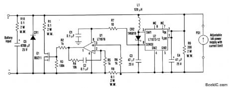
When developing a battery charger, using a real battery might be inconvenient. The battery simulator circuit described here is an alternative. The battery input positive and negative terminals should be connected in place of the battery in the charger circuit. Also, a current-limited lab-type power supply must be connected to the simulator circuit (as shown). In Discharge mode, the battery simulator uses the current-limited lab power supply PS1 as a source, and the simulator is inactive. In Charge mode, charge current is forced through the battery input terminals. Low voltage that develops across R8 is amplified by U1 and causes Q1 to shunt the charge current while maintaining the power-supply (PS1) voltage. U2, L1, CR2, C3, and C4 produce an internal 12-V power supply that is required to operate U1 and drive Q1. The PS1 voltage range is 1.5 to 15 V. Diode CR1 protects the circuit from reverse polarity and is needed if the maximum charge current is too high for the body diode of Q1 (Q1 must be heat sunk). R1 is a sense resistor for measuring the charge current. R10 and C5 simulate the ac characteristics of the battery. (View)
View full Circuit Diagram | Comments | Reading(3532)
MEASURING_PEAK_POWER
Published:2009/7/14 1:26:00 Author:May
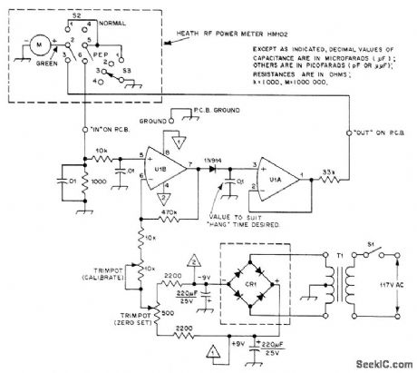
Addition of amplifier and rectifier circuits to Heath HM-102 or other similar RF wattmeter permits measurement of transmitter peak power output. DPDT toggle switch S2 is added to wattmeter to give choice of measurement desired. Circuit uses LM1458 or equivalent dual opamp. Current passing through 1N914 diode charges 0.1-μF capacitor at pin 3 of U1A, delaying meter return to zero long enough for reading of peak. When pointer just starts moving downward, next spoken word kicks it back up to peak value. To calibrate, set 10K pot so peak reading (S2 at PEP) is equal to normal reading (S2 at NORMAL) while using CW output of transmitter as test signal. CR1 is 2-A 50-PlV bridge rectifier. T1 has 12.6.V center-tap 100-mA secondary.-G. D. Rice, PEP Wattmeter-a la Heath, QST, Dee. 1976, p 30-3t. (View)
View full Circuit Diagram | Comments | Reading(3510)
7_W_FOR_QRP
Published:2009/7/14 1:24:00 Author:May
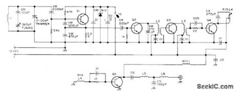
Operates at 7-W peak power for outing through interference when operating on low power on any CW band from 80 to 10 meters with typical inefficient antenna systems of portable operation, Q1 is 2N709 VFO feeding 2N697 amplifier a3 through 2N697 buffer Q2. Q4 is GE63 driver for Motorola HEP53001 final amplifier Q5. Keying can be introduced at Q2, Q3, or Q4. Article gives coil-winding data for all bands and covers construction and operation in detail. -J. Huffman, The Mini-Mite Allband QRP Rig, 73Magazine, Jury 1976, p 30-32 and 34-35. (View)
View full Circuit Diagram | Comments | Reading(855)
LOGICALLY_REDUNDANT_INVERTER
Published:2009/7/15 22:32:00 Author:Jessie
Symmetrical design with series-based diodes makes inverter independent of any single component failure.-T. Golstein, Reliable Circuits Through Redundancy, EEE, 11;3, p 56-59. (View)
View full Circuit Diagram | Comments | Reading(748)
| Pages:161/471 At 20161162163164165166167168169170171172173174175176177178179180Under 20 |
Circuit Categories
power supply circuit
Amplifier Circuit
Basic Circuit
LED and Light Circuit
Sensor Circuit
Signal Processing
Electrical Equipment Circuit
Control Circuit
Remote Control Circuit
A/D-D/A Converter Circuit
Audio Circuit
Measuring and Test Circuit
Communication Circuit
Computer-Related Circuit
555 Circuit
Automotive Circuit
Repairing Circuit