
Basic Circuit
Index 160
NiCd_BATTERY_CYCLER
Published:2009/7/14 2:07:00 Author:May
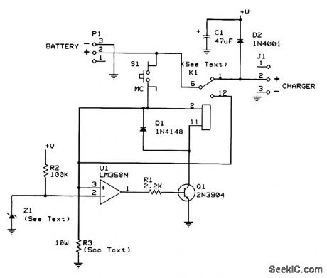
The battery cycler works with NiCd configurations of between three and nine cells. Cell combinations are accommodated by selecting Z1, K1, and R3 based upon the number of cells in the battery pack. This circuit is basically composed of a voltage comparator (U1), a voltage reference (Z1), and a switch (Q1 and K1). The op amp (U1) compares the reference voltage generated by the zener diode (Z1) and the battery. When the battery voltage matches (or is less than) the reference, the switch is turned off and the battery is allowed to charge. While the battery voltage is above the reference voltage, it is discharged through resistor R3. The resistor has been selected to discharge the battery at a rate between 200 and 300 mA. This rate keeps the power dissipation in R3 below 3 W and reduces the risk of opening any fuses in the battery circuitry located in the portable equipment. The push-button switch (S1) initiates the discharge process. If the battery voltage is below the reference when S1 is pressed, the unit will not discharge the battery because the lower operating limit of the battery has already been exceeded. If your batteries are in this condition, charge them for 18 hours and measure the voltage. If the batteries are still below the cutoff voltage, the problem is with one or more cells in the battery pack. (View)
View full Circuit Diagram | Comments | Reading(1545)
ZERO_CROSSING_HIGH_POWER
Published:2009/7/14 2:07:00 Author:May
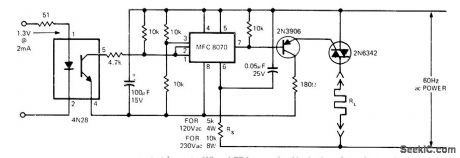
AC relay uses MFC8070 zero-voltage switch to provide gate current pulses for triac under control of differential input voltages derived from output of 4N28 optoisolator. When LED is off, voltage at pins 1 and 2 of switch is positive with respect to pin 3, inhibiting switch so no current pulses go to mac gate. When LED is energized by logic input, gate current pulses are generated at zero-voltage excursions of AC power source. Transistor ensures adequate gate drive at low temperatures. For normally-on configuration,interchange input connections 3 and 1-2 of switch. Triac can be selected to handle resistive loads from 4 to 40 A.-T. Mazur, Solid-State Relays Offet New Solutions to Many Old Problems, EDN Magazine, Nov. 20, 1973, p 26-32. (View)
View full Circuit Diagram | Comments | Reading(2404)
RING_COUNTER_WITH_VISUAL_READOUT
Published:2009/7/14 2:07:00 Author:May
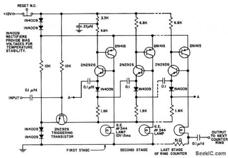
Uses only six components per stage. Combining of counter and indicator functions gives low battery drain. After reset button is re leased, 0.22-mid capacitor insures that first stage turns on. Current is drown by stage only when lamp is on. Any number of stages may be included in ring.- Transistor Manual, Seventh Edition, General Electric Co., 1964, p 203. (View)
View full Circuit Diagram | Comments | Reading(932)
1_kW_GROUNDED_GRID
Published:2009/7/14 2:07:00 Author:May
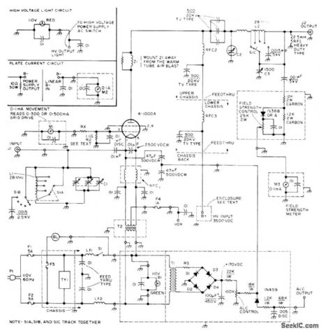
Class B linear amplifier for amateur transmitter can be switched to any band from 80 through 10 meters Do not exceed 200-mA grid drive, and do not apply full excitation without plate voltage. Tube requires blower for air cooling. Article covers construction and adjustment. -E, Hartz, 4-1000 A Grounded Grid Linear, 73 Magazine,July 1974, p 17, 19-20,22-24, and 26.
(View)
View full Circuit Diagram | Comments | Reading(2770)
450_470_MHz_AT_10_W
Published:2009/7/14 2:06:00 Author:May
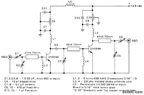
Power amplifier for land-mobile 12.5-V transmitter is constructed on double-sided microstrip substrate, Power gain at 470 MHz is 14.5 dB, and overall efficiency is 55%,-G. Young, UHF Microstrip Amplifiers Utilizing G-10 Epoxy-Glass Laminate, Motorola, Phoenix, AZ, 1976, AN-578, p 3. (View)
View full Circuit Diagram | Comments | Reading(890)
SWITCHING_4500_W_BELOW_5_kHz
Published:2009/7/14 2:05:00 Author:May
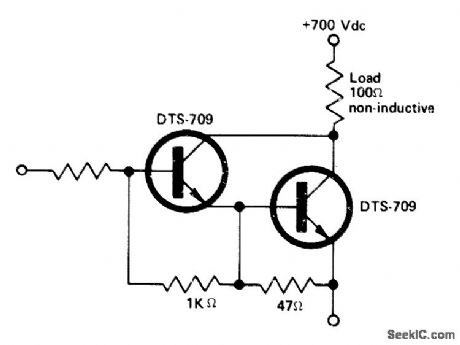
Simple Darlington connection of Delco DTS-709 transistors serves for switching of uρ to 700 V at 7A for low-speed motor control,regulator,and inverter applications.-″Low cost 'Dualithic Darlington'Switches 4500 Watts at up to 10 kHz,″ Deleo, Kokomo, IN, 1973, Application Note 54,p 3.
(View)
View full Circuit Diagram | Comments | Reading(1386)
BATTERY_IMPEDANCE_MEASURER
Published:2009/7/14 2:05:00 Author:May
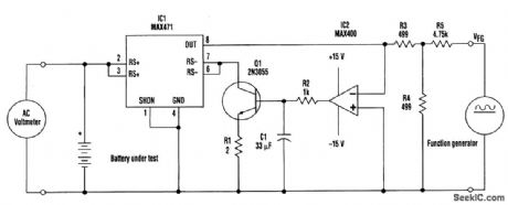
By applying an ac voltage superimposed on a ten times larger negative dc voltage (at VFG), the function generator determines the battery current drawn by Q1 (see the figure). The generator voltage causes the op-amp (IC2) output to go high and turn Q1 on, which allows battery current to flow through the high-side current-sensing amplifier (IC1). The output current of IC1, on pin 8, is equal to 1/2000 of this battery current. As a result, IC1, IC2, and Q1 form a loop in which the op amp forces a virtual ground at the IC1/IC2 end of R3. The op amp's extremely low-voltage offset (10 μV maximum) ensures accuracy. This virtual-ground condition enables the voltage divider (R5, and R3 in parallel with R4) and the function generator to determine the voltage across R3. The resulting current in R3 is iR3 = RP X VFG/【(RP+R5)R3】, where RP is the parallel combination of R3 and R4. Substituting resistor values and noting that battery current (iB) is 2000 times iR3,iB=-VFG/5.To operate the circuit, set the function generator's ac voltage to approximately 10 percent of its dc component. The equation then gives the resulting ac current in the battery (iB). Using an ac voltmeter, you can measure the ac voltage across the battery (vB) and calculate the average cell impedance as vB/NiB, where N is the number of cells. The circuit easily accommodates battery voltages of 3 V or more. (View)
View full Circuit Diagram | Comments | Reading(915)
RELAY_DRIVE
Published:2009/7/14 2:04:00 Author:May
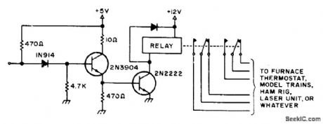
Logic input of 0 turns first transistor off, allowing base of next transistor to go high so it turns on and energizes relay for achieving desired control function.-D, D. Mickle, Practical Computer Projects, 73 Magazine, Jan. 1978, p 92-93. (View)
View full Circuit Diagram | Comments | Reading(856)
GEIGER_COUNTER_TO_IBM_INTERFACE
Published:2009/7/14 2:01:00 Author:May
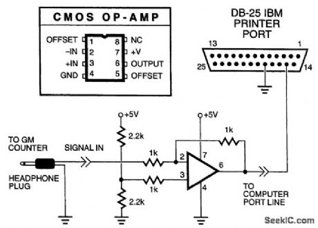
The simplest way to connect a Geiger counter to the IBM computer is to use a headphone jack to the parallel port. The headphone jack provides a +5- to 0-V pulse for each radioactive particle detected. The signal from the Geiger counter is +5 V. When radiation is detected, the signal pulses down to 0 V for a few milliseconds before returning to +5 V. Even though the signal is in the 0- to +5-V range, it is not safe to connect wires from an external circuit or instrument directly to the parallel-port lines without buffering. The op amp operates from a single-pole +5-V power supply. In this particular case, invert the signal from the Geiger counter. Because the pulse signals are +5 to 0 V, we do not require any amplification from our op amp. Therefore, the op arnp is configured as an inverting unity-gain follower. Remember that the Geiger counter outputs a steady +5V through the headphone jack. When it detects radiation, the output pulses down to 0 V for a few milliseconds. By inverting the Geiger counter signal with the op amp, the computer reads a steady 0 V on its line and a +5-V pulse when radiation is detected.
(View)
View full Circuit Diagram | Comments | Reading(1526)
VMOS_5_W_BROADBAND
Published:2009/7/14 1:59:00 Author:May
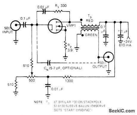
Single-transistor broadband linear amplifier uses Siliconix VMP1 to provide 15-dB gain over entire frequency range of 2 to 100 MHz.-G. D. Frey VMOS Power Amplifiers-This Broadband Circuit Outputs 8W with a 15 dB Gain, EDN Magazine. Sept 5, 1977, p83-85.
(View)
View full Circuit Diagram | Comments | Reading(933)
10_W_AT_450_MHz
Published:2009/7/14 1:56:00 Author:May
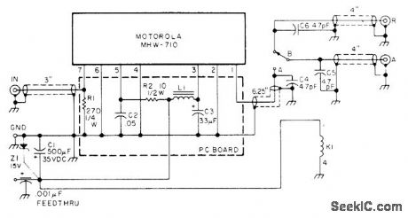
Uses Motorola MHW-710 sealed power module drawing 2.7 A on 13.8 VDC. Developed for use with fast-scan amateur TV transmitter having audio on video carrier and TR switching. Relay K1 is Archer (Radio Shack) 275-206. L1 is Ferroxcube VK200-201 4B.-B. J. Brown, Super Simple 450 MHz Rig, 73Magazine, Aug. 1976, p 72-75. (View)
View full Circuit Diagram | Comments | Reading(1283)
SHUNT_PIN_DIODE_RF_SWITCH
Published:2009/7/14 1:56:00 Author:May
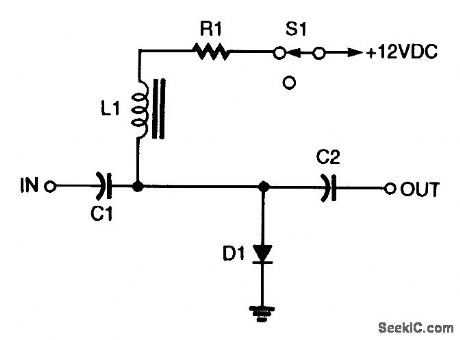
D1 is a PIN diode (MV3404) used as a switch, with dc bias supplied via R1 and L1.This shunt PIN-diode switching circuit directs signals to ground when D1 is forward-biased. (View)
View full Circuit Diagram | Comments | Reading(1387)
SOLID_STATE_STROBOSCOPE
Published:2009/7/14 1:53:00 Author:May
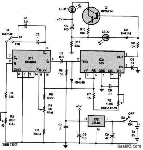
The schematic diagram for the stroboscope is shown. When switch S2 is closed, a 9-V battery B1 is connected to IC3, a 78L05 voltage regulator, which provides a 5-V source to the circuit. Capacitors C8 and C9 filter the supply. A CD4046 phase-locked loop, IC1, provides a low-frequency square wave to the circuit. Potentiometer R4-a 5000-Ω,10-turn, precision potentiometer with a built-in turns counter-provides a way to adjust and get a direct readout of the FPM rate from 0 to 1000. Switch S1 lets you select the multiplier affecting that rate. Setting S1 to×1, therefore, gives you a 0- to 1000-FPM range, whereas setting S1 to ×10 results in a 0- to 10,000-FPM range. The values of the multiplier settings are determined by capacitors C1 and C2. A 555 timer, IC2, configured in a monostable mode, provides a pulse with a width that is adjustable via R8. That audio-taper potentiometer allows the duration or pulse width to be varied from 10 μs at the minimum setting to 1000μs at the maxi-mum setting. An MPSA14 Darlington transistor, Q1, is configured as a capacitive- discharge -type cur-rent sink, which provides an approximately 90-mA pulse (for the pulse duration set by R8) through LED1, the flash output. The super-bright LED specified for LED1 has a maximum rating of 100 mA.. (View)
View full Circuit Diagram | Comments | Reading(3005)
BATTERY_CAPACITY_INDICATOR
Published:2009/7/14 1:52:00 Author:May
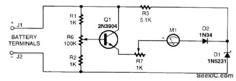
Zener diode D1 creates a reference voltage to which the battery voltage is compared. The diode specified has a breakdown voltage of 5.1 V. That rating will work fine with most six- or seven-cell NiCd battery packs, as well as with 12-V lead-acid batteries. The circuit can be customized for a particular battery by selecting a unit for D1 that has a voltage rating about 1 V below the completely discharged voltage of the battery pack that you wish to measure. Transistor Q1, an emitter-follower amplifier, greatly increases the sensitivity of the circuit over what it would be if R7 were connected directly to the wiper of R6. A further advantage to that arrangement is that it reduces the current drain that flows through RI, R2, and R6. By amplifying the current flowing through the resistors, the resistance value can be increased to a very high value, lowering the total current draw of the circuit. Resistor R6 adjusts the meter to read 0 mA when the battery is completely discharged and R7 adjusts the meter to read 1 mA when the battery is fully charged. If the circuit were accidentally connected backward to the battery, current would flow through D1 and M1. The transistor would become re-verse-biased, allowing a complete path back to the battery. That situation would allow excessive current to flow through D1, M1, and Q1, destroying them in the process. D2, R1, and R2 are included to prevent any current flow in case the battery is reversed. (View)
View full Circuit Diagram | Comments | Reading(1107)
COIN_TOSS_CIRCUIT
Published:2009/7/14 1:51:00 Author:May
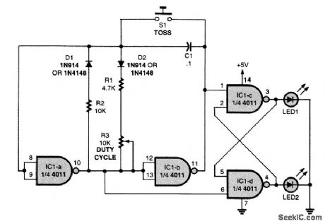
Shown is a CMOS coin-toss circuit that works well and can be built with a single 4011 or 4001 CMOS IC.(Note that the IC pin numbers in the diagram apply for both the 4001 and the 4011.) Two gates form a clock, and the others make up a bistable multivibrator. With this circuit ,It is necessary to adjust the 10,000-Ω potentiometer (R3) for a 50-percent duty cycle. If you don’t have a scope to do this, simply measure the direct current flowing through each LED while adjusting R3. When the same current level flows through each LED, the clock will be adjusted for a 50-percent duty cycle. (View)
View full Circuit Diagram | Comments | Reading(2824)
VFO_FOR_7_AND_14_MHz
Published:2009/7/14 1:48:00 Author:May
Drift rate of Seiler variable-frequency oscillator can be less than 100 Hz if reasonable care is taken in board design and parts selection. Oscillator Q1 is followed by buffer stages Q2 and Q3. Tuning control R1 varies DC voltage applied to varactor tuning diode. Developed for use with 1-W exciter as solid-state transmitter for low-power (QRP) operation in 40-meter and 20-meter bands. VFO runs continuously to enhance stability; if oscillator signal leaks through receiver and interferes with desired incoming signal, switching S1 to RECEIVE puts R4 in circuit to move oscillator from operating frequency. Offset resistor R4 can also serve for improving band spread on 20 meters.-A. Weiss, QRP, CQ, Dec. 1977, p 88-92 and 112.
(View)
View full Circuit Diagram | Comments | Reading(2023)
100_W_LINEAR_FOR_432_MHz
Published:2009/7/14 1:46:00 Author:May
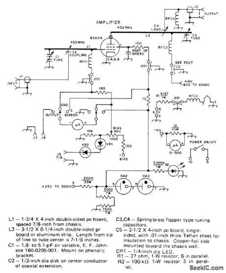
Medium-powered amplifier using 8560A conduction-cooled tetrode provides extra power needed for use of Oscar satellite in mode B on 432.15 MHz, with drive of only 7 W. Half-wave grid is fabricated from double-sided printed-circuit board. Capacitive probe to grid line serves for input coupling. Half-wave plate line is capacitively tuned by movable vanes. Article covers construction in detail.-T. McMullen, A Tramplifier for 432 MHz, QST, Jan. 1976, p 11-15. (View)
View full Circuit Diagram | Comments | Reading(922)
FREEZE_FRAME_STROBE
Published:2009/7/14 1:45:00 Author:May
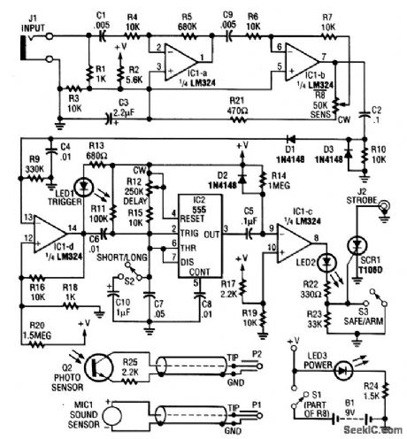
A sensor input from a mike or photodetector is amplified and used to trigger an SCR, which, in turn, triggers a camera strobe. This circuit is useful for freeze-frame photos of phenomena, such as drops of water, explosions, shots, etc. (View)
View full Circuit Diagram | Comments | Reading(811)
MINI_ROULETTE
Published:2009/7/14 1:42:00 Author:May
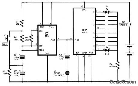
A circuit diagram for a mini battery-powered version of roulette is shown, This circuit uses a 4017 decade counter (IC2) driving 10 LEDs. Because only one LED is ever illuminated at any one time, a common limiting resistor R4 is used. They can also be placed in alternating red/green order for added effect. The counter IC2 is clocked by IC1, a classic 555 timer connected as an astable.When the SPIN button is pressed and then released, full speed is achieved, and then the display gradually slows down until it stops on a single number. Capacitor C2 governs the oscillator speed, and resistor R3 prevents instability when the LED rotation stops. The piezo disk transducer, X1, is placed on the output of the oscillator to provide a sound effect. (View)
View full Circuit Diagram | Comments | Reading(3427)
DUAL_MODE_BATTERY_LIFE_EXTENDER
Published:2009/7/14 1:42:00 Author:May
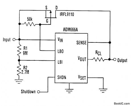
Most voltage regulators stop functioning when the differential voltage between the input and output is reduced below a certain level. At this level, the regulator's output voltage begins to drop at an accelerated rate, resulting in a much lower voltage's being available to the circuit. To prevent this from happening, the battery voltage is monitored and a low-battery warning signal is issued, indicating the approaching end of battery life. In the circuit presented here, the voltage regulator is bypassed when a low battery level is detected-the battery is connected directly to the circuit. At high battery voltage levels, the output voltage is regulated by the linear regulator, and the low-battery indicator (LBI) comparator output is off. Also, the LB0 pin is pulled to Vbatt (input), keeping the power MOSFET off. As the input voltage drops and approaches the regulator's dropout voltage, the base current to the regulator's pass transistor reaches its maximum, turning it on very hard. Lowering the input voltage any further will result in art increase in the pass transistor's saturation voltage and a reduction in the regulator's output voltage. The input level detector's crossover voltage should be set to Vout + Vsat of the pass transistor. When the input voltage falls below the crossover point, the comparator output is turned on. This pulls the gate voltage to ground, which turns on the power MOSFET. From this point, the voltage available to the circuit is the battery voltage minus the voltage across the power FET, which is insignificant. (View)
View full Circuit Diagram | Comments | Reading(776)
| Pages:160/471 At 20141142143144145146147148149150151152153154155156157158159160Under 20 |
Circuit Categories
power supply circuit
Amplifier Circuit
Basic Circuit
LED and Light Circuit
Sensor Circuit
Signal Processing
Electrical Equipment Circuit
Control Circuit
Remote Control Circuit
A/D-D/A Converter Circuit
Audio Circuit
Measuring and Test Circuit
Communication Circuit
Computer-Related Circuit
555 Circuit
Automotive Circuit
Repairing Circuit