
Basic Circuit
Index 147
5_MHz_COAX_LINE_DRIVER
Published:2009/7/14 4:37:00 Author:May
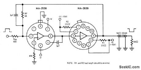
Combination of Harris HA-2530 wideband inverting amplifier and HA-2630 unity-gain current amplifier pro-vides 20-dB gain with extremely high slew rate and full power bandwidth even under heavy output loading conditions.- Linear & Data Acquisition Products, Harris Semiconductor, Melbourne, FL, Vol. 1, 1977, p 2-47-2-50. (View)
View full Circuit Diagram | Comments | Reading(708)
100_1_FREQUENCY_RANGE
Published:2009/7/14 4:37:00 Author:May
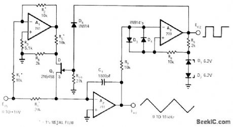
Circuit provides good stability and excellent linearity over wide operating range. For values shown and +15 V supply, circuit transfer function is about t kHz/ V over 100:1 frequency range, with linearity error less than 0.5%. Although circuit does not have sine-wave output, triangle output is easily converted to sine wave by filtering to remove harmonics. Article traces circuit operation.-G. Bank, A Wideband, Linear VCO, EDN/EEE Magazine, July 15, 1971, p 49-50. (View)
View full Circuit Diagram | Comments | Reading(802)
DECOUPLING_FOR_PULSE_DELAY
Published:2009/7/15 3:39:00 Author:Jessie
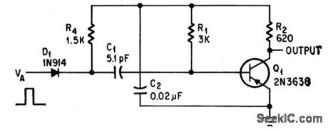
Coupling circuit ahead of input-inverting digital pulse delay prevents C1 from loading driving collector and decreases noise sensitivity.-R. A.Karlin, One-Transistor Multi Delays Digital Pulses, Electronics, 38:17, p 85-86. (View)
View full Circuit Diagram | Comments | Reading(726)
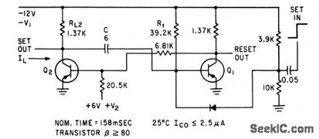
INTEGRATOR_OF_SOLID_STATE_PHANTASTRON
Published:2009/7/15 3:38:00 Author:Jessie
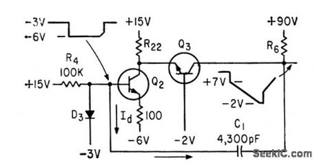
Q2 and Q3 provide open-loop gain, while R4 and C1 are feedback elements.-S. R. Parris and D. A Staar, Highly Accurate Phantastron Delay Circuit, Electronics, 33:43, p 72-74. (View)
View full Circuit Diagram | Comments | Reading(699)
TONE_BURST_GENERATOR
Published:2009/7/15 3:37:00 Author:Jessie

One section of 556 dual timer is connected as mono MVBR and other section as oscillator. Pulse established by mono turns on oscillator, allowing generation of AF tone burst.- Signetics Analog Data Manual, Signetics, Sunnyvale, CA, 1977, p 723-724. (View)
View full Circuit Diagram | Comments | Reading(3361)
FOUR_QUADRANT_SIGNAL_MULTIPLIER
Published:2009/7/15 3:36:00 Author:Jessie
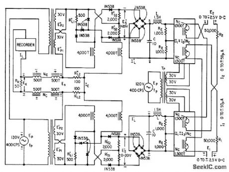
Highspeed magnetic-amplifier square-law circuits with silicon diodes and resistors replace slow-response thermal converters in. four-quadrant analog multiplying device. Polarity-reversible signal currents I1 and I2 cre multiplied with two square-law and two push-pull magnetic amplifier circuits. Reversible-polarity output drives ink oscillograph. -W. A. Geyger, Multiplying Circuit Uses Magnetic Amplifiers, Electronics, 32:2, p 58-59. (View)
View full Circuit Diagram | Comments | Reading(1983)
SUBAUDIO_T0_20_MHz
Published:2009/7/15 3:36:00 Author:Jessie
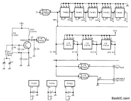
Square-wave signal source covers wide frequency range in fully tunable decade steps, as TTL signal source for experimentation with counters, microprocessors, and other logic circuits. Uses tunable 2N2222 transistor oscillator operating at 10-20 MHz, with switchable decade dividers for range selection and switchable binary dividers for band selection. Article covers construction and calibration,-A. G. Evans, Digital Signal Source, 73 Magazine, Dec. 1977, p 150-151.
(View)
View full Circuit Diagram | Comments | Reading(1128)
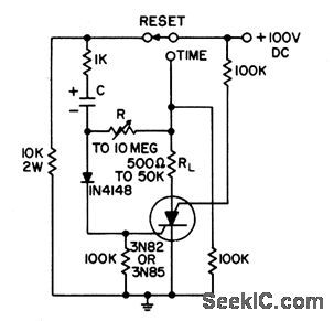
A_C_OPERATED_TIME_DELAY
Published:2009/7/15 3:03:00 Author:Jessie
Switch is normally closed, charging C and blocking scs.Delay is initiated by opening switch. After delay interval, determined by R, Q, and potenliometer, silicon controlled switch conducts on altenate half-cycles. Transistor Manual, Seventh Edition, General Electric Co., 1964, p 435. (View)
View full Circuit Diagram | Comments | Reading(773)
THREE_PHASE_PULSE_GENERATOR
Published:2009/7/15 3:03:00 Author:Jessie
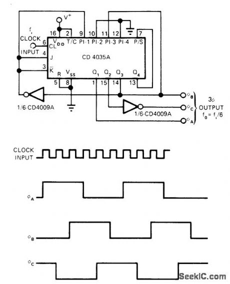
Requires only CMOS 4-bit shift register and two CMOS inverters. Register is connected to operate as divide-by-6 Johnson counter giving glitch-free outputs. Circuit is driven by square-wave clock signal having frequency 6 times that of desired output frequency.-C. Rutschow, Simple CMOS Circuit Generates 3-Phase Signals, EDN Magazine, June 20, 1976, p 128. (View)
View full Circuit Diagram | Comments | Reading(3269)
CONVENTIONAL_MONO_MVBR
Published:2009/7/15 3:02:00 Author:Jessie
Requires bulky capacitors and large timing resistors to get accurate delay times of 1 to 300 millisec. Ideal for laboratory use, but gives problems with mass production.-D.E. Haselwood. Monostable Multivibrators with Stable Delay Times. Electronics.34:49,p64-65 (View)
View full Circuit Diagram | Comments | Reading(731)
LOAD_CURRENT_DELAY
Published:2009/7/15 3:01:00 Author:Jessie
Silicon controlled switch circuit delays start of load current for interval of 0.5 RC after switch is thrown.- Transistor Manual, Seventh Edition, General Electric Co. 1964, p 435. (View)
View full Circuit Diagram | Comments | Reading(897)
500_MC_TO_1000_Mc_DOUBLER
Published:2009/7/15 3:01:00 Author:Jessie
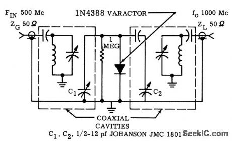
Single varactor gives up to 15 w output from 25 w input, with output linear up to 11 w. Conversion efficiency is 50%.-G. Schaffner and J. Cochran, Varactor Diodes and Circuits for High Power Output and linear Response, Motorola Application Note AN-191, Aug.1965. (View)
View full Circuit Diagram | Comments | Reading(805)
1215_MC_TO_243_MC_DOUBLER
Published:2009/7/15 3:00:00 Author:Jessie
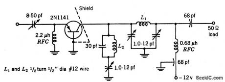
Input is tuned to fundamental and output to second harmonic. Combination series-parallel trap in collector circuit rejects fundamental.-Texas Instruments Inc., Transistor Circuit Design, McGraw-Hill, N.Y., 1963, p 328. (View)
View full Circuit Diagram | Comments | Reading(630)
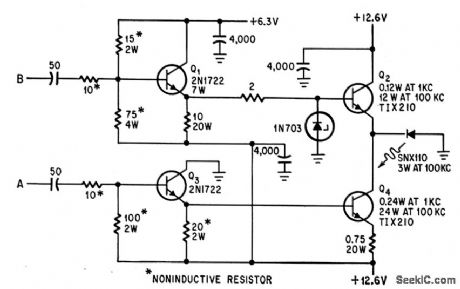
INTERFACES_FOR_100_OHM_LINE
Published:2009/7/14 4:25:00 Author:May
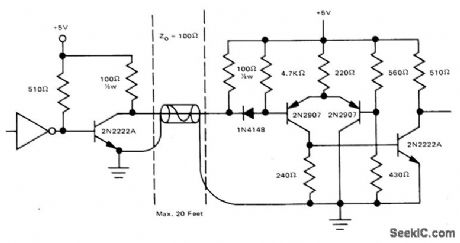
Permits transferring data signals from SA900/901 diskette storage drive to location of MC6800 microprocessor up to maximum of 20 feet away through 100-ohm coax. Data line drivers used are capable of sinking 100-mA in logic true state with maximum voltage of 0.3 V with respect to logic ground. When line driver is in logic false state, driver transistor is cut off and voltage at output of drive( is at least 3 V with respect to logic ground.- Microprocessor Applications Manual (Motorola Series in Solid-State Electronics), McGraw-Hill, New York, NY, 1975, p 5-211-5-212. (View)
View full Circuit Diagram | Comments | Reading(735)
8_BIT_PROGRAMMABLE_INPUT
Published:2009/7/14 4:24:00 Author:May
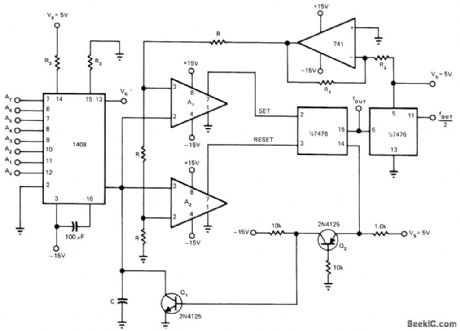
Serves as digitally programmable frequency source covering 10 to 2550 Hz for systems under microprocessor control. Frequency change is essentially instantaneous, assuring immediately valid data. Uses MC1408L8 8-bit monolithic D/A converter to supply constant current for charging C in negative direction. When capacitor voltage exceeds lower negative threshold voltage at pin 3 of LM311 high-impedance comparator A1, comparator changes state and sets 7476 flip-flop.This turns on Q1 through level-shifter Q2, discharging C until it exceeds higher threshold voltage at pin 2 of A2. Flip-flop then resets and C begins charging again. Second half of 7476 serves as divider. To cover above frequency range, values should be: R3.9K; R1 27K; R2 10K; R3 2.2K; C 0.1 μF. Circuit gives 8-bit accuracy. Design equations are presented in article.-A. Helfrick, Eight-Bit Frequency Source Suited for μP Control, EDN Magazine, Sept. 20, 1976, p 116 and118. (View)
View full Circuit Diagram | Comments | Reading(1643)
RECEIVE_FILTER
Published:2009/7/14 4:30:00 Author:May
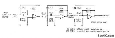
Used as prefilter having controlled group-delay distortion, ahead of receiving modem in data transmission system. Values shown are for 950-1400 Hz answer filter. For 1900-2350 Hz originate filter, change critical values to those given in parentheses. -D. Lancaster, TV Typewriter Cookbook, Howard W. Sams, Indianapolis, IN, 1976, p 180-182. (View)
View full Circuit Diagram | Comments | Reading(901)
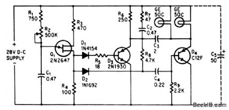
SCR_CONTROLS_PHOTOFLASH
Published:2009/7/14 4:29:00 Author:May
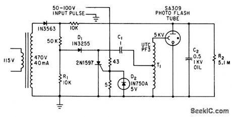
C1 is charged to 100 v by ac power supply. Input trigger pulse fires 2N1597 scr to make C1 discharge through primary of T1. Peak of 5 kv in secondary triggers photoflash. Maximum repetition rate is 20 flashes per second.-E. L. Harris, Jr., Solid ,State Components Shrink Photoflash Control, Electronics, 36:15, p 70. (View)
View full Circuit Diagram | Comments | Reading(707)
DRIVER_FOR_UGHT_DIODE
Published:2009/7/14 4:26:00 Author:May
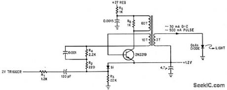
When blocking oscillator is triggered, its output controls flashes from light-emitting diode. Triple-winding transformer gives maximum output for minimum power-supply drain.-C. H. Moulton, Light Pulse System Shrinks High-Voltage Protection Device, Electronics, 38:11, p 71-75. (View)
View full Circuit Diagram | Comments | Reading(843)
50_DUTY_CYCLE
Published:2009/7/14 4:26:00 Author:May

Provides 80 flashes per minute. Scr's conduct alternately in parallel inverter with capacitor commutation, and are triggered by free-running relaxation oscillator Q1. Flashing rate is determined by R1-R2-C1.-D. V. Jones, Quick-On-The-Trigger Design, Electronics, 38:12, p 105-110. (View)
View full Circuit Diagram | Comments | Reading(821)
LOCKED_90°OUTPUTS
Published:2009/7/14 4:26:00 Author:May
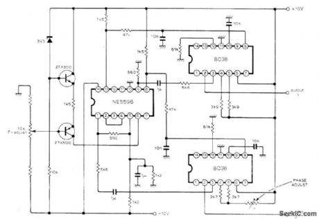
Delivers two-phase (sine and cosine) outputs locked together. Frequency can be varied over wide range by altering bias current with 10K pot that produces common-mode output voltage in NE5596 multiplier IC driving 8038 ICs serving as VC0s. Triangular outputs of oscillators are fed to multiplier inputs for phase control. Lower-cost 566 VCO can be used if sinusoidal outputs are not needed. Phase error over tuning range is nominally zero, whereas with conventional phase locked loop circuitry the capture range may be exceeded or phase error can be large.-J. M. Worley, Two-Phase V. C.O., Wireless World, Dee. 1976, p 41.
(View)
View full Circuit Diagram | Comments | Reading(1108)
| Pages:147/471 At 20141142143144145146147148149150151152153154155156157158159160Under 20 |
Circuit Categories
power supply circuit
Amplifier Circuit
Basic Circuit
LED and Light Circuit
Sensor Circuit
Signal Processing
Electrical Equipment Circuit
Control Circuit
Remote Control Circuit
A/D-D/A Converter Circuit
Audio Circuit
Measuring and Test Circuit
Communication Circuit
Computer-Related Circuit
555 Circuit
Automotive Circuit
Repairing Circuit