
Basic Circuit
Index 153
HALL_MULTIPLIER_FOR_ANALOG_RATIO_COMPUTER
Published:2009/7/15 4:08:00 Author:Jessie
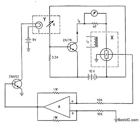
Indium arsenide Hall plate serves as analog multiplier in circuit with photoresistor R and 2N174 grounded-emitter power amplifier that controls drive current of Hall generator. Differential amplifier A in feedback loop including lamp I controls Hall current. -H. H. Wieder, Analog Ratio Computer Uses Hall Multiplier, Electronics, 36:45, p 46-47. (View)
View full Circuit Diagram | Comments | Reading(1311)
SMOOTHED_D_C_FROM_F_M
Published:2009/7/15 4:08:00 Author:Jessie
Mean d-c level, derived from f-m data on magnetic tape, undergoes R-C smoothing in three-transistor pulse-counting demodulator circuit so output can be fed to cro.-K.R. Whittington, Simple F-M Demodulator for Audio Frequencies, Electronics, 35:48, p89. (View)
View full Circuit Diagram | Comments | Reading(1632)
SQUARE_ROOT_OF_SUM_OF_SQUARES_OF_THREE_VARIABLES
Published:2009/7/15 4:06:00 Author:Jessie
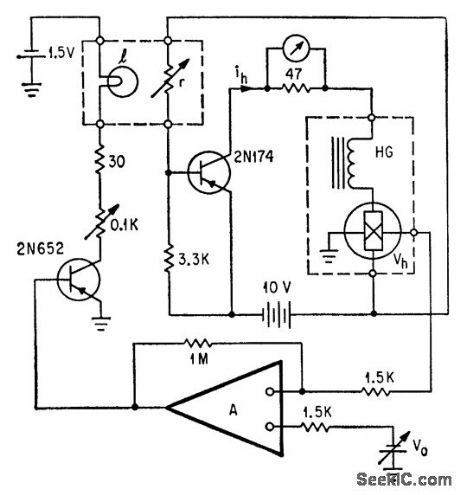
Output signal of Hall-effect squaring multiplier HG is fed to differential amplifier A. Amplified difference controls current through lamp that determines resistance of photoresistor r which, with 2N174, controls Hall current derived from voltage source.-H. H. Wieder, Square-Root Computer Uses Hall Multiplier, Electronics, 37:4, p 30-31. (View)
View full Circuit Diagram | Comments | Reading(984)
UJT_LED_PULSER
Published:2009/7/15 4:01:00 Author:Jessie
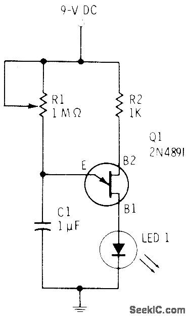
Rise time of output pulse is about 200 ns and width is about 25 μs when using 1 μF for C1. Reducing value of C1 reduces pulse width. C1 charges through R1 until voltage across C1 is high enough to bias UJT into conduction. C1 then discharges through UJT and LED and cycle repeats. LED can be any common type.-F. M. Mims, Electronic Circuit book 5:LED Projects, Howard W. Sams, Indianapolis,IN, 1976, p 30-32. (View)
View full Circuit Diagram | Comments | Reading(902)
100_W_AT_50_KC
Published:2009/7/15 4:00:00 Author:Jessie

Square-wave oscillator Q1-Q2 drives monostable gates Q3-Q5 and Q4-Q6 in parallel, and gates in turn drive push-pull amplifier using 25-amp transistorsQ7-08 lo deliver 100 w to load al 50 kc with overall efficiency of 70%.-S. L. Chin, New Circuit Design Raises Inverter Frequency Limits, Electronics, 35:43, p 59-60. (View)
View full Circuit Diagram | Comments | Reading(751)
EXTENDED_RANGE_ASTABLE
Published:2009/7/15 3:59:00 Author:Jessie
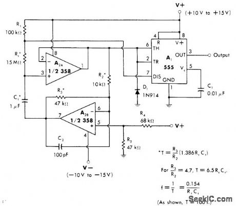
Square-wave output is extended in frequency by combining buffer A2A with opamp A2B functioning as capacitance multiplier for 555 timer connected as astable MVBR,Value of 1-μF timing capacitor Ct is increased in effective value by ratio of gain of A2B stage, equal to R3/R2. Output frequency thus corresponds to that of 4 7-μF capacitor, Negative supply should be equal and opposite to positive supply.-W. G. Jung, IC Timer Cookbook, Howard W. Sams, Indianapolis, IN,1977, p118-121. (View)
View full Circuit Diagram | Comments | Reading(813)
OUTPHASED_TONE_GENERATOR
Published:2009/7/14 3:47:00 Author:May
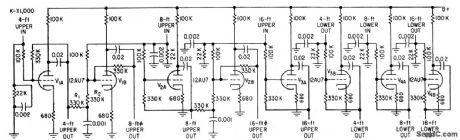
Bus amplifiers located between keying-system outputs and formant filters provide outphosed signals that lack even-harmonic content. Combinations of these produce organ lone colors called for by voicing panel.-R. H. Dorf, Electronic Organ Uses Neon Tone Generators, Electronics, 31:35, p 36-411. (View)
View full Circuit Diagram | Comments | Reading(836)
HIGH_LINEARIT_PHASE_DEMODULATOR
Published:2009/7/15 3:59:00 Author:Jessie
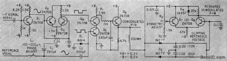
I-f signal is amplified by Q1, clipped by Q2-Q3,and resulting square wave phase-demodulated in coincidence Circuit,Q4-Q5 which also receives similarly clipped 455-kc reference signal. Demodulated output of Q6 is reshaped by clipper Q7-Q8, to give symmetrical output with linearity for deviations up to 85 deg.-W. H. Casson and C. C. Hall, New Phase-Tracking Demodulator Will Not lock on Sidebands, Electronics, 36:6, p 52-55. (View)
View full Circuit Diagram | Comments | Reading(750)
UNIVERSAL_TELEPHONE_HOLDING_CIRCUIT
Published:2009/7/14 3:46:00 Author:May
If you have Touch-Tone telephone service, you can put a call on hold from any phone in your house by plugging this simple device into any telephone jack. The universal hold circuit works with any phone that has a keypad with a # key. To put a call on hold, press the # key and hang up the phone. A timer extends the #-key function while you hang up phones that have a keypad built into the handset. The universal hold circuit first detects the dual-tone, multifrequency (DTMF) signal that is generated when the # key is pressed. It then activates a circuit that partially loads the telephone line so that the central office thinks a phone is still off-hook-even after it is hung up. The hold circuit remains active for 5 seconds after the # key is released, so the key does not have to be held down while the phone is being hung up. When any phone is again picked up, the hold function is canceled. (View)
View full Circuit Diagram | Comments | Reading(1807)
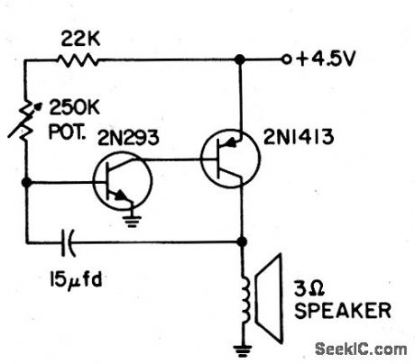
TWO_TRANSISTOR_METRONOME
Published:2009/7/14 3:46:00 Author:May

Rheostat provides rate adjustment.- Transistor Manual, Seventh Edition, general Electric Co.,1964, p 379. (View)
View full Circuit Diagram | Comments | Reading(868)
ELECTRONIC_ORGAN_FREQUENCY_DIVIDER
Published:2009/7/14 3:45:00 Author:May
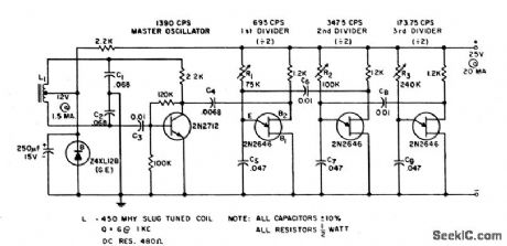
Ujt relaxation oscillator circuits reduce number of master oscillators needed and eliminate large inductors.- J. F. Cleary and D. V. Jones, A Unijunction Frequency Divider, EEE, 12:5, p 52-53. (View)
View full Circuit Diagram | Comments | Reading(1770)
SYNCHRONOUS_DEMODULATOR_FOR_COHERENT_PULSE_DOPPLER_RADAR
Published:2009/7/15 3:57:00 Author:Jessie
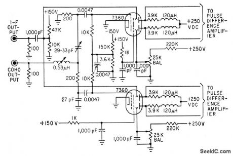
C-w output of coherent oscillator is applied to control grid of one beam-defection tube, and radar re ceiver i-f output is applied to control grid of other tube in push-pull, so i-f signal and modulation products are in push-pull at the two anodes while c-w signal components are in same phase and are hence cancelled in following pulse difference amplifiers.-J. B. Theiss, More Target Data with Sideband Coherent Radar, Electronics, 36:3, p 40--43. (View)
View full Circuit Diagram | Comments | Reading(1026)
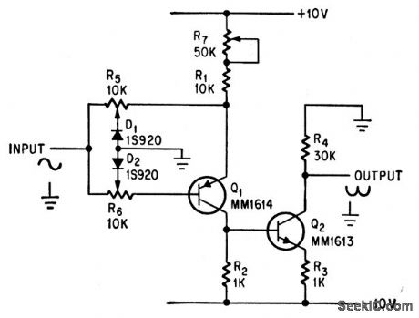
CURRENT_REGULATOR
Published:2009/7/14 3:45:00 Author:May
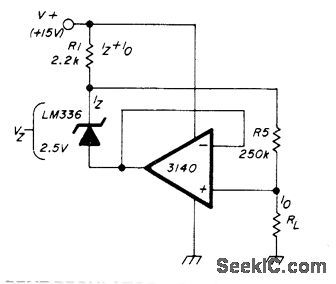
Combines zener with opamp in bootstrap configuration. Regulated output current lO can be any value less than lz but must be much greaterthan opamp bias current. Current in zener is set by R1 to provide minimum of 1 mA. Performance can be improved by using Motorola MC1403 or other 2.5-V three-terminal voltage reference in place of zener. -W. Jung, AnIC Op Amp Update, Ham Radio, March 1978, p 62-69. (View)
View full Circuit Diagram | Comments | Reading(829)
AF_SQUARE_WAVES
Published:2009/7/15 3:57:00 Author:Jessie

With value shown for C1, frequency of output square wave is 530 Hz. For 5300 Hz, use 0.001 μF; for 53 Hz, use 0.1 μF. Circuit will drive ordinary crystal earphone or crystal microphone used as earphone.-F. M. Mims, Integrated Circuit Projects, Vol. 5, Radio Shack, Fort Worth, TX, 1977, 2nd Ed., p 52-56.
(View)
View full Circuit Diagram | Comments | Reading(751)
NEON_OSCILLATOR_SYNCHRONIZER
Published:2009/7/14 3:44:00 Author:May
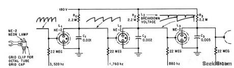
Metal clips on neon lamps are used to synchronize successive stages of neon-lamp relaxation oscillators, overcoming their inherent instability. Used in frequency-division type of electronic organ tone generator.-R. F. Woody, Jr., Clip Couples Neon Oscillators, Electronics, 39:9, p 77. (View)
View full Circuit Diagram | Comments | Reading(1496)
TRANSFORMERLESS_FULL_WAVE_DETECTOR
Published:2009/7/15 3:56:00 Author:Jessie
Each half-cycle of input sine wave produces negative half-cycle at output. Both input and output are referenced to ground. Operating range is from d-c to 10 Mc.-C. Yarker. Full-Wave Detector Without Transformer.Electronics.39:15,p100-101. (View)
View full Circuit Diagram | Comments | Reading(846)
AF_RF_SQUARE_WAVE
Published:2009/7/15 3:55:00 Author:Jessie
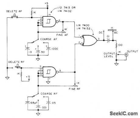
Use of feedback resistor between input and output of each gate produces oscillation in each Schmitt-trigger oscillator, one operating at audio frequencies and one operating at radio frequencies. Both AF and RF can befed into NAND gate to give modulated RF, or outputs can be used separately as clocks for microprocessor.-B. Grater and G. Young, Build a Pulse Generator, Kilobaud, June 1977, p49. (View)
View full Circuit Diagram | Comments | Reading(1830)
BILATERAL_CURRENT_SOURCE
Published:2009/7/14 3:41:00 Author:May
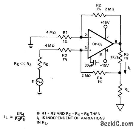
Output current through load is constant within 2% of value related to input voltage and resistor values, regardless of variations in load from 10 to 2000 ohms. Circuit is built around Precision Monolithics OP-08 opamp.- Precision Low Input Current Op Amp, Precision Monolithics, Santa Clara, CA, 1978, OP-08, p 7. (View)
View full Circuit Diagram | Comments | Reading(2724)
PUSH_PULL_OUTPUT
Published:2009/7/14 3:41:00 Author:May
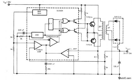
Transformer-coupled push-pull output for SG3524 fixed-frequency pulse-duration- modulated switching regulator gives output flexibility, allowing for multiple outputs and wide range of output voltages. Each output transistor operates alternately at half of switching frequency. Switching regulator applies voltage alternately to opposite ends of transformer primary, making transformer perform as if it had AC input. TIP101A rectifier then provides desired 5-VDC output at 5A.-J. Spencer, Monolithic Switching Regulators-They Fit Today's Power-Supply Needs, EDN Magazine, Sept. 5, 1977, p 117-121. (View)
View full Circuit Diagram | Comments | Reading(1514)
2_KC_SCR_INVERTER
Published:2009/7/15 5:03:00 Author:Jessie
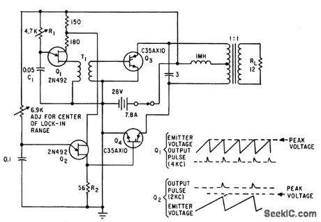
Circuit shows parallel inverter, but unijunction relaxation oscillators Q1and Q2 could also trigger series inverter, giving symmetrical operation. Q1 operates at twice the frequency of Q2.-D. V. Jones, Turn-Off Circuits for Controlled Rectifiers, Electronics, 33:32, p 52-55. (View)
View full Circuit Diagram | Comments | Reading(1465)
| Pages:153/471 At 20141142143144145146147148149150151152153154155156157158159160Under 20 |
Circuit Categories
power supply circuit
Amplifier Circuit
Basic Circuit
LED and Light Circuit
Sensor Circuit
Signal Processing
Electrical Equipment Circuit
Control Circuit
Remote Control Circuit
A/D-D/A Converter Circuit
Audio Circuit
Measuring and Test Circuit
Communication Circuit
Computer-Related Circuit
555 Circuit
Automotive Circuit
Repairing Circuit