
Basic Circuit
Index 154
ORGAN_SWELL_SHOE
Published:2009/7/14 3:40:00 Author:May
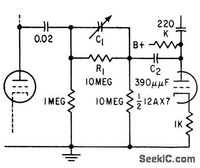
Uses capacitive volume control C1 to replace expensive industrial-type potentiometer. Operation of swell shoe varies value of C2 which consists of two hinged metal plates. C1 is series leg of capacitive voltage divider, shunt leg of which is dynamic capacitance of about 0.02 mfd across tube grid due to capacitive feedback from plate through C2. Attenuation range is great, and noise and hum cue negligible.-R. H. Dorf, Electronic Organ Uses Neon Tone Generators, Electronics, 31:35, p 36-41. (View)
View full Circuit Diagram | Comments | Reading(735)
D_C_FROM_F_M
Published:2009/7/15 3:55:00 Author:Jessie
Mean d-c level, directly proportional to number of pulses per unit time, is read on meter for f-m data recorded on magnetic tape.-K. R. Whittington, Simple F-M Demodulator for Audio Frequencies, Electronics, 35:48, p 89. (View)
View full Circuit Diagram | Comments | Reading(789)
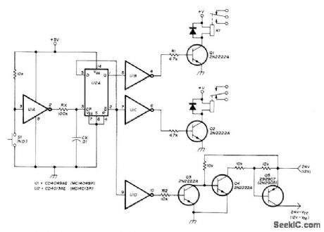
PROGRAMMABLE_ASTABLE
Published:2009/7/14 3:40:00 Author:May
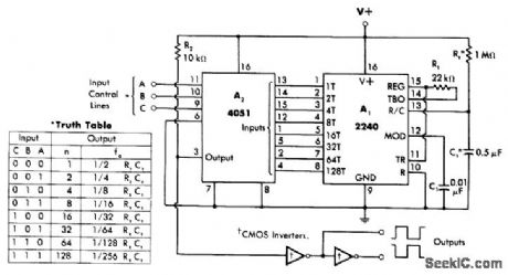
Square-wave output frequency of Exar XR-2240 programmable timer/counter is made digitally programmable by use of 4051 CMOS multiplexer having three-line channel-select control ABC, Lines select one of eight possible switching paths by binary combination. When all three inputs are zero, highest of eight basic output frequencies of 2240 is obtained, as shown in truth table. Circuit will yield outputs with periods of 1, 2, 4, 8, 16, 32, 64, and 128 s. -W. G. Jung, IC Timer Cookbook, Howard W. Sams, Indianapolis, IN, 1977, p 123-125. (View)
View full Circuit Diagram | Comments | Reading(0)
PHASE_SENSITIVE_DEMODULATOR_1
Published:2009/7/15 3:49:00 Author:Jessie
Operates over range of 1kc to 20 Mc without need for tuning. In phase-locking applications, both inputs may be single-ended. Output voltage is proportional to phase difference between input signals.-H. F. Strenglein, Phase Demodulator Needs no Tuning, Electronics, 38:20, p 99. (View)
View full Circuit Diagram | Comments | Reading(949)
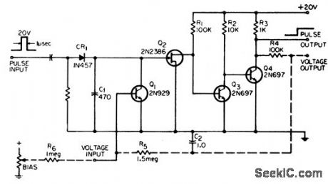
LOAD_CURRENT_TURNOFF_DELAY
Published:2009/7/15 3:42:00 Author:Jessie
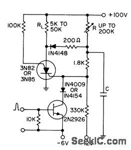
Input pulse turns off silicon controlled switch, which triggers after delay of approximately RC.- Transistor Manual, Seventh Edition, General Electric Co. 1964, p 435. (View)
View full Circuit Diagram | Comments | Reading(621)
MONOSTABLE_MVBR_DELAY
Published:2009/7/15 3:40:00 Author:Jessie
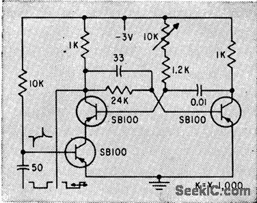
Prevents certain circuits from operating until proper time and generates and shapes required output pulses. Is triggered by positive pulse produced by input differentiating circuit. Circuits are cascaded, and second stage starts its delay coincident with trailing edge of first delay output pulse.-W. W. Grannemann et al, Pulse. Height-to-Digital Signal Converter, Electronics, 33:2, p 58-60. (View)
View full Circuit Diagram | Comments | Reading(721)
ANSWERING_MACHINE_MESSAGE_STOPPER
Published:2009/7/14 3:39:00 Author:May
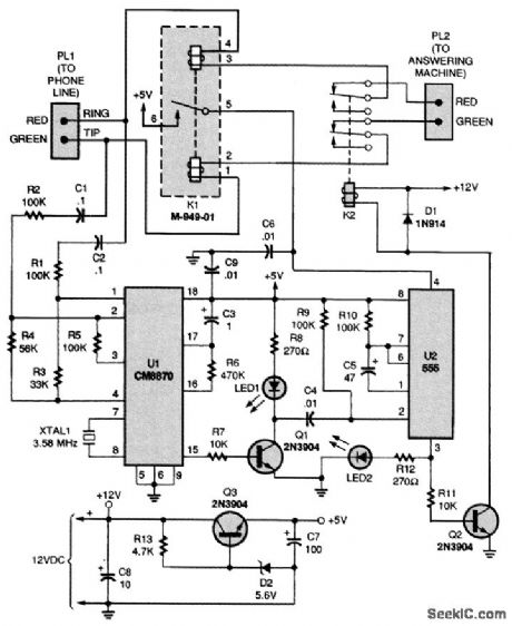
The message stopper connects between your present answering machine and any convenient modular phone jack. When any extension telephone on the same line rings and the answering machine answers the phone first, you can easily stop the outgoing message and reset the machine for the next call simply by pressing a key on the tone-dialed telephone's keypad. The schematic diagram for the message stopper is shown. Power for the circuit is supplied by a 12-V source. It is fed to the junction of K2 and Dl, also dropped to 5 V through a voltage-regulator stage composed of Q3, resistor R13, and zener diode D2, and fed to the balance of the circuit. Plug PL1 connects to the telephone line. The tip and ring conductors of that plug are connected in series to line-sense relay K1, line-disconnect relay K2, and finally plug PL2, which connects to the answering machine. Integrated circuit U1, a CM8870 DTMF receiver, monitors the phone line for the presence of DTMF signals. That chip contains an internal op-amp stage that allows it to be interfaced to the phone line using only a pair of capacitors (C1 and C2) and a few resistors. The voltage gain of the internal amplifier is unity in this circuit. When a connected answering machine answers the line and a DTMF signal is detected by U1, the output at pin 16 of U1 goes high. That causes capacitor C3 to begin discharging through resistor R6. The output at pin 15 goes high. A DTMF tone pair must be present before pin 15 goes high approximately 1/3, second and is determined by the following formula t 0.67RC where r is the time in seconds, R is the value of R6 in ohms, and C is the value of C3 in farads. As the output of pin 15 goes high, Q1 is turned on, lighting LED1 and triggering the 555 timer U2, configured as a monostable multivibrator, into operation via C4. However, U2 can receive power only if the answering machine answers the line. That is accomplished by the relay contacts within line-sense relay K1 applying +5 V to pin 4 of U2. Once U2 is triggered, pin 3 goes high for approximately 5 seconds, LED2 illuminates, and Q2 switches on. Relay K2 switches on; disconnecting the answering machine from the phone line for approximately 5 seconds. That should give the typical answering machine time to detect the line disconnection and force it to reset for the next call. However, the length of the time period can be altered by changing the values of R10 or C5, as shown in the formula: t =RC, where f is the time in seconds, R is the. value of R10 in ohms, and C is the value of C5 in farads. (View)
View full Circuit Diagram | Comments | Reading(2407)
BATTERY_REGULATOR
Published:2009/7/14 3:39:00 Author:May
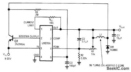
Uses LM376N positive voltage regulator in switching mode to compensate for voltage changes of battery sup-ply during discharge cycle, without adjusting series rheostat. Load regulation is 0.3% for un-regulated input of 9 to 30 V, with R1 and R2 setting output voltage anywhere between 5 and 27 V. Maximum output current is 25 mA. Switching frequency of regulator is 33 kHz. -E. R. Hnatek and L. Goldstein, Switching Regulator Designed for Portable Eqiupment, EDN|EEE Magazine, Sept. 15, 1971, p 39-41. (View)
View full Circuit Diagram | Comments | Reading(1032)
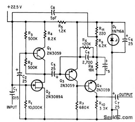
RECORDING_PHOTOMULTIPLIER_OUTPUT
Published:2009/7/14 3:36:00 Author:May
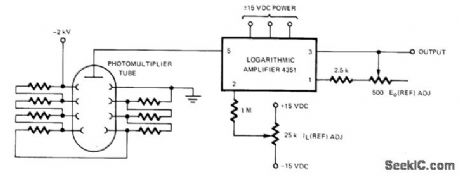
Wide range of output data from photomultiplier is fed through Teledyne Philbrick 4351 logarithmic amplifier for compression of data to range of ±5VDC for feed to tape recorder. Report covers calibration procedure for obtaining overall accuracy of ±2 dB.- How to Specify Parameters of Nonlinear Circuits, Teledyne Philbrick, Dedham, MA, 1974, AN-15, p 4. (View)
View full Circuit Diagram | Comments | Reading(757)
CLOSED_LOOP_REGULATOR_FOR_INDUCTION_HEATER
Published:2009/7/14 3:35:00 Author:May
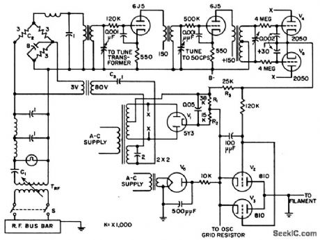
Switching action is performed by parallel triodes V2 and V3 that replace 5,000 ohms of oscillator grid resistance. Tungsten-lamp bridge serves as measuring circuit that produces phase-modulated supply-frequency error signal. Requires no components with heavy power rating because only low-power signal is required by switching triode.-J. Markus, Handbook of Electronic Control Circuits, McGraw-Hill, N.Y., 1959, p 178. (View)
View full Circuit Diagram | Comments | Reading(1048)
TONE_BURST_CIRCUIT
Published:2009/7/14 3:35:00 Author:May
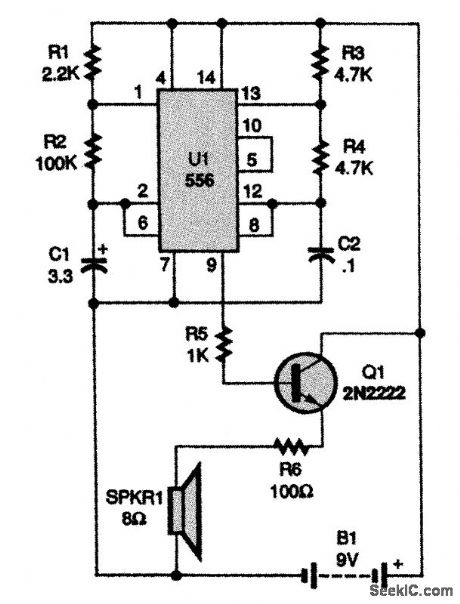
The tone-burst circuit puts out a 500-Hz tone, at a rate of 1 Hz, through an 8-Ω speaker, SPKR1. Besides the 9-V battery and its connecting snap, SPKR1 is the only non-surface-mount component in the circuit. The circuit can also be built from standard-size components. (View)
View full Circuit Diagram | Comments | Reading(971)
0_12_V_PROGRAMMABLE
Published:2009/7/14 3:34:00 Author:May
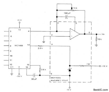
Combination of Motorola MC1408 DAC and MC1723 regulator gives digitally programmable voltages in 0.1-V increments at currents in excess of 100mA. Can be used as programmable lab power supply, computer-controlled supply for automatic test equipment, or in industrial control systems. Requires ±5 V and ±15V supplies. Voltage range can be increased to 25.5 V if positive supply is increased to 28.5 V or higher.-D. Aldridge and N. Wellenstein, Designing Digitally-Controlled Power Supplies, Motorola, Phoenix, AZ, 1975, AN-703, p 3. (View)
View full Circuit Diagram | Comments | Reading(1079)
LOGARITHMIC_RATIO
Published:2009/7/14 3:31:00 Author:May
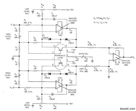
Output is proportional to logarithm of ratio of input voltages V1 and V2 for voltages between 0 and 10 V. Each input goes to modified logamp circuit using Analog Devices 180K. Outputs are combined by differential opamp (Analog Devices 184L), with Fairchild μA726 temperature -regulated dual transistor serving asfeedback element. Amicle gives design equations and analyzes possible error sources.-D. R. Morgan, Get the Most Out of Log Amplifiers by Understanding the Error Sources, EDN Magazine, Jan. 20, 1973, p 52-55. (View)
View full Circuit Diagram | Comments | Reading(1061)
PHASE_LOCK
Published:2009/7/15 20:48:00 Author:Jessie
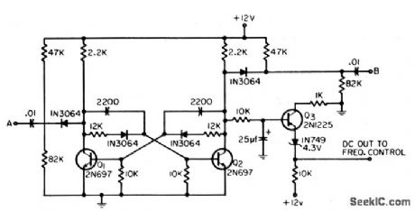
Uses flip-flop, filter, and d-c level shift to phase-lock low-frequency oscillator to a desired frequency. Trigger from master frequency source is fed in at B, and trigger from phase-locked frequency is fed to A. Used to sync ujt sawtooth generator to operate at 10 times the 16-cps center frequency at B.-H. Anway, Phase-locked Frequency Discriminator, EEE, 14;3, p 61. (View)
View full Circuit Diagram | Comments | Reading(811)
TWO_STAGE_A_F_DISCRIMINATOR
Published:2009/7/15 20:43:00 Author:Jessie
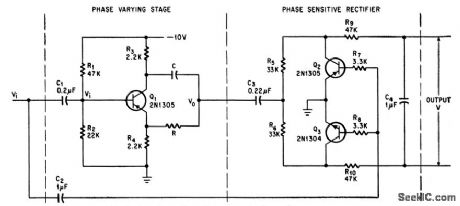
Circuit first shifts phase of incoming signal in proportion to its frequency deviation, then produces d-c voltage proportiotml to phase shift. Used to measure wow and fluller of disk and tape recorders having prerecorded audio signal.-J. F. Delpech, Audio Discriminator Measures Lctrge Frequency Changes, Electronics, 39:9, p 76-77. (View)
View full Circuit Diagram | Comments | Reading(851)
MONO_AND_PRE_DISCRIMI_NATOR
Published:2009/7/15 20:41:00 Author:Jessie
Monoslable multivibrator can be electronically adjusted to vary output pulse width over range of 0.2 microsec to several seconds. By adding feedback path shown in dashed lines, circuit also serves as pulse repetition frequency discriminator in which d.c output voltage is function of frequency front 3 cps to 300 kc.-G. Richwell, Widedlange Monostable, PRF Discriminator, EEE, 13:8, p67. (View)
View full Circuit Diagram | Comments | Reading(645)
PHASE_DISCRIMINATOR_FOR_A_C_BRIDGE
Published:2009/7/15 20:39:00 Author:Jessie
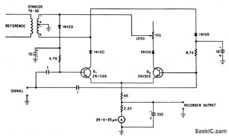
Amplifed output of cc bridge is compared with ctc reference signal. When both are in phcse, d-c output to recorder is maximum of one polarity. For 180°phase difference, output is maximum of opposite polarity, and is zero for phase-quadrature.-W. A. Rhine-hart and L. Mourlam, FET Performs Well In Balancing Act, Electronics, 38:19, p 88-92 (View)
View full Circuit Diagram | Comments | Reading(947)
CHANNEL_SELECTOR_REPLACES_TUNING_DEVICES
Published:2009/7/15 20:36:00 Author:Jessie
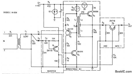
By sensing leading edges of input signal, discriminator having two monostable multivibrators, inverter, and two and gates provides output for desired channel frequency in radio, television, telemetry, and digital control systems.-J. H. Firestone, Gated Pulses Yield Selected Frequency Outputs, Electronics, 36:51, p 38-40. (View)
View full Circuit Diagram | Comments | Reading(694)
PTT_LATCH
Published:2009/7/14 3:29:00 Author:May
Eliminates need for holding down microphone switch continuously while transmitting. U1 is inverting hex buffer, and U2 is dual CM0S D flip-flop. When S1 is depressed, input to U1A goes low and its output goes high, making U2A and U1B together turn on Q2 and energize relay K1. Q3-Q5 serve as optional silent power switch for use when relay noise is objectionable.-B. Lambing, DC Latch Circuit, Ham Radio, Aug. 1975, p 42-44. (View)
View full Circuit Diagram | Comments | Reading(1001)
SAMPLER_AND_MULTIPLEXER
Published:2009/7/14 3:29:00 Author:May
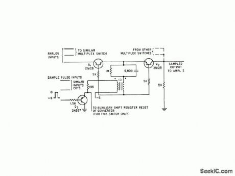
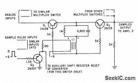
Sample of signal input voltage is fed to output when sampling pulse from external digital timing matrix is applied to primary of pulse transformer through Q3.-N. Aron and C. Granger, Analog-To-Digital Converter Uses Transfluxors, Electronics, 35:20, p 62-66. (View)
View full Circuit Diagram | Comments | Reading(869)
| Pages:154/471 At 20141142143144145146147148149150151152153154155156157158159160Under 20 |
Circuit Categories
power supply circuit
Amplifier Circuit
Basic Circuit
LED and Light Circuit
Sensor Circuit
Signal Processing
Electrical Equipment Circuit
Control Circuit
Remote Control Circuit
A/D-D/A Converter Circuit
Audio Circuit
Measuring and Test Circuit
Communication Circuit
Computer-Related Circuit
555 Circuit
Automotive Circuit
Repairing Circuit