
Basic Circuit
Index 146
GAIN_PROGRAMMABLE
Published:2009/7/14 4:41:00 Author:May
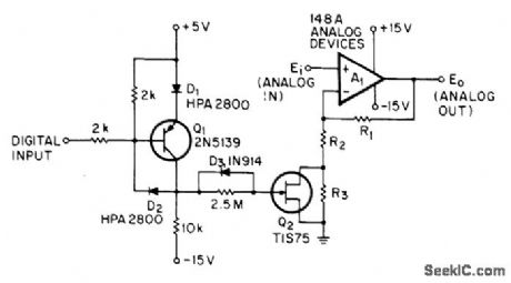
Gain of non-inverting opamp can be programmed with standard digital logic levels. With input at 0 V, Q1 is turned on but is held out of saturation by Schottky diode D2. Resulting opamp gain is (R1 + R2)/R2.If R2 is 1.13 kilohms and R1 10 kilohms, gain is 10. When input is 5 V, Q1 is off and gate of Q2 is driven to -15 V. Gain now becomes (R1 + R2 + R3)/(R2 + R3). If R3 is 8.87 kilohms, gain is 2.-K. Karash, Gain-Programmable Amplifier, EEE Magazine, Sept. 1970, p 89. (View)
View full Circuit Diagram | Comments | Reading(1070)
FLASH_TIMER
Published:2009/7/14 4:35:00 Author:May
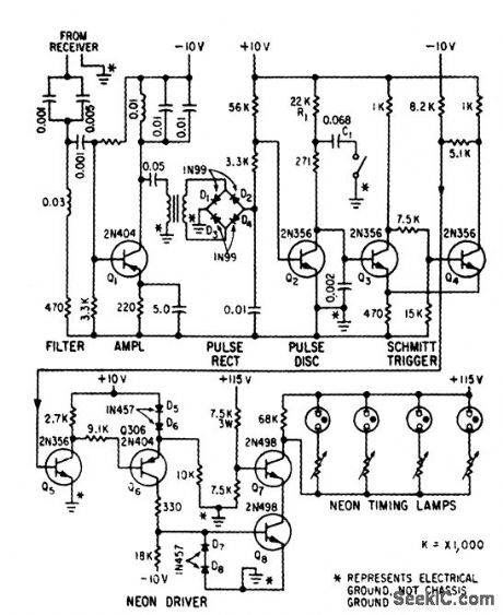
Provides properly synchronized flash illumination for cameras in response to subcarrier pulse commands from uhf receiver.-F. M. Gardner and L. R. Hawn, Camera Control System for Rocket Sled Tests, Electronics, 33:14, p 63-65. (View)
View full Circuit Diagram | Comments | Reading(635)
POLARITY_REVERSING_SPLIT
Published:2009/7/14 4:34:00 Author:May
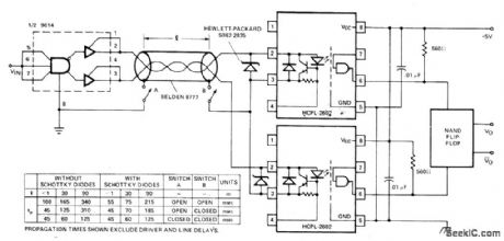
PHASE DRIVE-Half of 9614 polarity-reversing line driver feeds pair of Hewlett-Packard HCPL-2602 optically coupled line receivers through coax cable. Cable-grounding switches A and B change performance Closing only switch B enhances common-mode rejection but reduces propagation delay slightly. Closing both switches optimizes data rate. Schottky diodes at receiver inputs improve data rate, NAND flip-flop at output greatly improves system noise rejection in split-phase termination of line.- Optoelectronics Designer's Catalog 1977, Hewlett-Packard, Palo Alto,CA,1977,p158-159. (View)
View full Circuit Diagram | Comments | Reading(966)
CONSTANT_CURRENT_REGULATOR
Published:2009/7/14 4:33:00 Author:May
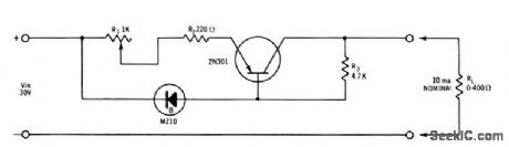
Uses transistor ad variable series resistor. Current will remain within 10% of 10 ma from short circuit up to maximum load of 400 ohms. - Zener Diode Handbook, International Rectifier Corp., 1960, p59. (View)
View full Circuit Diagram | Comments | Reading(1130)
±15_V_TRACKING
Published:2009/7/14 4:39:00 Author:May
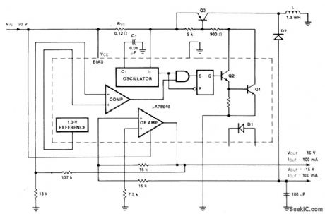
Dual-tracking connection for Fairchild μA78S40 switching regulator operates from single 20-V input Efficiency is 75% for+15 V and 85% for -15 V, both at 100 mA. Output ripple is 30 mV.-R. J. Apfel and D. B. Jones, Universal Switching Regulator Diversifies Power Subsystem Applications, Computer Design, March t978, p 103-112, (View)
View full Circuit Diagram | Comments | Reading(2218)
FUNCTION_GENERATOR
Published:2009/7/15 3:13:00 Author:Jessie
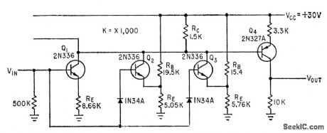
Desired function of input voltage is developed across RC and inverted by Q4. One application is for computing ground range of radar target front slant range. Transistors eliminate need for d-c amplifier.-D. R. Chick, Boosting Function Generator Output with Transistors, Electronics, 33:13, p 75-76. (View)
View full Circuit Diagram | Comments | Reading(6045)
SQUARE_LAW_OUTPUT
Published:2009/7/15 3:12:00 Author:Jessie
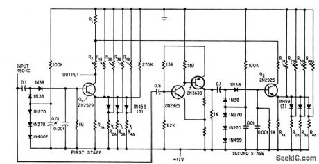
Diode network and detector provide output proportional to square of input voltage. Input range of 40 db is split into two 20-db segments. Each stage saturates and gives constant output for voltages above operating range. For voltages below operating range, stage is cut off and has zero output. Combination of two stages gives desired square-law characterisitic. Resistor values are: R1A, R3A a=3.18K,R1B=57.9K, R3B=18.75K, R5 =3K、R7=10, R2A, R4B =5.06K, R4A =0.86K, R2B =64.2K,R6 = 300 and R8, R9 = 990.-R. J. Matheson, Square-Law Defector has 40-db Dynamic Range, Electronics, 39:18, p 95-97. (View)
View full Circuit Diagram | Comments | Reading(1147)
FAST_SYNCHRONIZING
Published:2009/7/14 4:38:00 Author:May
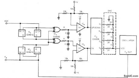
Combination of phase splitter and DAC provides accurate synchronization of high-stability VCO with external reference frequency. IC divides reference frequency by 4 and provides two signals 90° apart, while IC2 divides VC0 frequency similarly by 4. Phase relationship between outputs of IC3 depends on whether VCO is higher or lower than reference, while frequency of IC3 outputs depends on difference between oscillator and reference frequencies, Schmitt triggers IC4 and IC5 supply clock and up/down control to counter IC6. If VC0 frequency is low, IC6 counts up at rate proportional to frequency difference and delivers increasing control voltage to VCO as required for increasing oscillator frequency.-H. W. Cooper, Oscillator Synchronizer Is Fast Acting, EDN Magazine, July 20, 1973, p 83-84. (View)
View full Circuit Diagram | Comments | Reading(1262)
PHOTOELECTRIC__FUNCTION__GENERAIOR
Published:2009/7/15 3:11:00 Author:Jessie
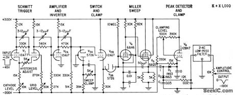
Open-loop photoelectric function generator generates any single-value function With 1%accuracy, as required for duplicating particular antenna patterns in radar simulator. Uses horizontal sweep of 10 millisec (100 cps) with 5-kc vertical sweep.-B. Silverberg, Function Generator for Radar Simulator, Electronics, 32:2, p 52-55. (View)
View full Circuit Diagram | Comments | Reading(787)
Q_MULTIPLIER_FOR_TONE_FILTER
Published:2009/7/15 3:11:00 Author:Jessie
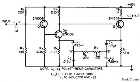
Provides stable multiplication over wide temperature range, as required for high-selectivity singlefrequency telemetry tone filter. Center frequency is 8 kc and bandwidth is 40 cps. Q is about 200.-W. New, Jr., Stable Q Mulliplier, EEE, 13:4, p 41. (View)
View full Circuit Diagram | Comments | Reading(725)
TV_TURNOFF_WITH_WARNING_BEEP
Published:2009/7/15 3:10:00 Author:Jessie
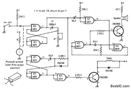
Timer providing turnoff delays up to 1 h gives warning beep about 30 s before turnoff to permit resetting if desired for watching remainder of particular program. Can be mounted inside TV set or in small chairside box connected to set by cable. Photocell can be substituted for ON/OFF switch to permit remote control with flashlight while leaving entire circuit in TV set. Can be operated from 9-V battery if this voltage is not available in receiver. Momentary closing of switch turns on TV and initiates timing cycle. With 3.6-megohm pot for R, maximum delay is 1 h. For 30-min delay, use 1.3 megohms. Setting of R determines exact delay.-J. Sandier, 9 Projects under $9, Modern Electronics, Sept. 1978, p 35-39. (View)
View full Circuit Diagram | Comments | Reading(776)
PROGRAMMABLE_GAIN
Published:2009/7/14 4:38:00 Author:May

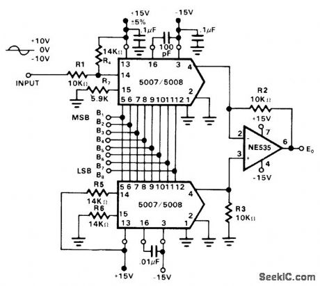

Combination of two Signetics 5007/5008 multiplying D/A converters and NE535 opamp gives digital control of attenuation and gain in audio system. AC input controls polarity of output, giving output of ±10 V for inputs from DC to 10 kHz and ±5 V if response goes up to 20 kHz.- Signetics Analog Data Manual, Signetics, Sunnyvale, CA, 1977, p 677-685. (View)
View full Circuit Diagram | Comments | Reading(767)
FAST_RECYCLING_TIME_DELAY_RELAY
Published:2009/7/15 3:10:00 Author:Jessie
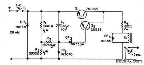
Uses 28-V relay to give delay of 5 sec, with recycle time of 200 millisec. -R.W. Eubank. Fast Cycling Time-Delay.EEE.12:3,p71 (View)
View full Circuit Diagram | Comments | Reading(847)
VARIABLE_SINE_COSINE_FUNCTION_GENERATOR
Published:2009/7/15 3:10:00 Author:Jessie
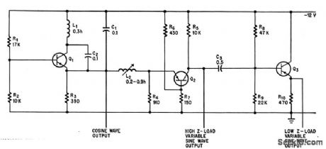
For testing phase detector, one output gives reference cosine function and other gives waveform that can be varied in phase from sine to cosine function, with choke of high or low output impedance. Q1 is modified Colpitts. Frequency stability is 1% from 1 kc to 100 kc with regulated power supply.-J.G. Peddie, Oscillator Generates Sine, Cosine Waves Simultaneously, Electronics,37:22, p 74. (View)
View full Circuit Diagram | Comments | Reading(903)
AUDIO_FET_SQUARING_CIRCUIT
Published:2009/7/15 3:09:00 Author:Jessie
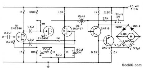
Used in noise investigation, analog computation, and measurement of power in complex wave-forms, where squarer of high accuracy and wide bandwidth is required. First stage is phase divider whose outputs drive squaring fet's Q2 and Q3 Output of squarer is coupled through capacitor to meter rectifier whose reading is Proportional to square of amplitude of input voltage.-L. J. Sevin, Jr., Field-Effect Transistors, McGraw-Hill, N.Y., 1965, p 83. (View)
View full Circuit Diagram | Comments | Reading(738)
PRECISION_SCR_DELAY
Published:2009/7/15 3:08:00 Author:Jessie
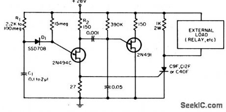
Gives time delays over 3 minutes without need for tantalum or electrolytic capacitor. Timing capacitor C1 can be mylar unit. Application of power in itiates timing of power, which is determined by R1-C1. Al end of interval, 2N494C fires other scr, to place supply voltage across load.-D. V. Jones, Precision Solid-State Delay Circuit, EEE, 11:12, p 26-27. (View)
View full Circuit Diagram | Comments | Reading(676)
TUNNEL_DIODE_TIME_DELAY
Published:2009/7/15 3:06:00 Author:Jessie
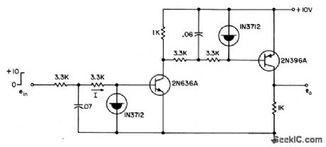
Uses two cascaded complementary stages in which tunnel diodes are used with transistors. Takes +10V input pulse.- Transistor Manual, Seventh Edition, General Electric Co. 1964, p 369. (View)
View full Circuit Diagram | Comments | Reading(850)
5_HR_TIME_DELAY
Published:2009/7/15 3:05:00 Author:Jessie
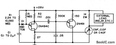
Range of 0.3 millisec to 5 hours is obtained without using electrolytic capacitor. At end of timing interval, initiated by applying power and determined by R1-C1, 2N494C triggers controlled rectifier- Transistor Manual, Seventh Edition, General Electric Co. 1964, p 322. (View)
View full Circuit Diagram | Comments | Reading(728)
_24_V_FROM__12_V_AT_2_A
Published:2009/7/14 4:37:00 Author:May
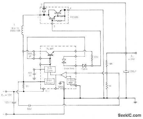
Combination of PIC635 boost switching regulator and TL497 control circuit accepts DC input voltage and provides regulated output voltage that must be greater than input voltage. When transistor switch is turned on, input voltage is applied across L. When transistor is turned off, energy stored in L is transferred through diode to load where it adds to energy transferred directly from input to output during diode conduction time, Output voltage is regulated by controlling duty cycle.- Flyback and Boost Switching Regulator Design Guide, Unitrode, Watertown, MA, 1978, U-76, p 9. (View)
View full Circuit Diagram | Comments | Reading(691)
FREQUENCY_DOUBLED_OUTPUT
Published:2009/7/15 3:05:00 Author:Jessie
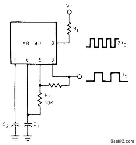
Current-controlled oscillator section of Exar XR-567 tone decoder is connected to double frequency of square-wave output by feeding portion of output at pin 5 back to input at pin 3 through resistor. Quadrature detector of IC then functions as frequency doubler to give twice output frequency at pin 8. Supply voltage range is 5-9 V.- Phase-Locked Loop Data Book, Exar Integrated Systems, Sunnyvale, CA, 1978, p 41-48. (View)
View full Circuit Diagram | Comments | Reading(3280)
| Pages:146/471 At 20141142143144145146147148149150151152153154155156157158159160Under 20 |
Circuit Categories
power supply circuit
Amplifier Circuit
Basic Circuit
LED and Light Circuit
Sensor Circuit
Signal Processing
Electrical Equipment Circuit
Control Circuit
Remote Control Circuit
A/D-D/A Converter Circuit
Audio Circuit
Measuring and Test Circuit
Communication Circuit
Computer-Related Circuit
555 Circuit
Automotive Circuit
Repairing Circuit