
Basic Circuit
Index 148
WAVEFORM_EDGE_PULSER
Published:2009/7/15 3:34:00 Author:Jessie
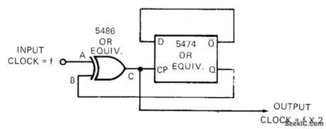
Circuit generates square-wave output pulse for each edge of square-wave input. EXCLUSIVE-OR gate is used as programmable inverter that returns point C to quiescent low state following each transfer of data through 5474 IC. When used for frequency-doubling, input waveform should be symmetrical because output is proportional to propagation delay of flip-flop plus delay of 5486 EXCLUSIVE-OR gate.-D. Giboney, Double-Edge Pulser Uses Few Parts, EDN Magazine, Dec. 15, 1972, p 41. (View)
View full Circuit Diagram | Comments | Reading(930)
POWER_SWITCH_FOR_SWITCHING_REGULA_TOR
Published:2009/7/14 4:23:00 Author:May
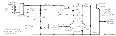
Circuit operating from 12-V step-down transformer includes push-pull driver providing interface between logic drive signal and 2N6306 high-voltage power transistor. Switching is provided at 3 A and 20 kHz, with artificial negative bias supply created from single positive supply to improve fall time. Current limiting is added to base current to limit overdrive and reduce storage time. Power switch is turned off by forcing IC to logic low. Used in 24-V 3-A switching-mode power supply operating from AC line.- R. J. Haver, A New Approach to Switching Regulators, Motorola, Phoenix, AZ, 1975, AN-719,p5. (View)
View full Circuit Diagram | Comments | Reading(835)
TEMPERATURE_TO_FREQUENCY_CONVERTER_CIRCUIT
Published:2009/7/14 4:23:00 Author:May
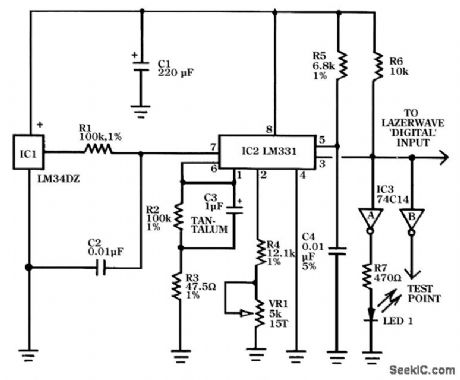
IC1 produces the Fahrenheit-dependent voltage at its output. This is fed into the LM331 VFC through precision resistor R1. Inside IC2 are a switched current source, an input comparator, and a one-shot timer. The input comparator is designed to produce a trigger pulse if the voltage at pin 7 is greater than the voltage at pin 6. It does this by comparing the two voltages, one of which is generated internally by the switched current source, and the other of which is obviously the input. The switched current source charges capacitor C3. When the comparator trips and produces its trigger pulse, it activates the monostable multivibrator, which outputs a positive pulse that turns on the out-put transistor. The monostable multivibrator turns on the switched current source for a period of 1.1 times RC, where RC is the combination of resistor R5 and capacitor C4. C1 charges up to a point where it exceeds the input voltage, and the comparator resets itself; thus the frequency output transistor Q1 will be turned off. Resistor R2 discharges C3 in a time interval that depends on the values of both components. Then, the input comparator and monostable multivibrator are reset, and an-other cycle will be implemented as long as there is sufficient input voltage. Finally, resistors R4 and VR1 set the amount of current the constant-current source is able to inject into C3. Thus, VR1 can set the response span of the IC by adjusting it. 103, two gates of a hex Schmitt trigger, are used to buffer IC2's output to light an LED and to make available a digital signal, Remember two things about IC3: Its logic 1 output will be a full9V, not the TTL level of 5 V, and all unused inputs must be tied to ground to prevent self-oscillation at RF frequencies and consequent malfunction of the circuit. (View)
View full Circuit Diagram | Comments | Reading(1476)
FAST_SETTLING_COAX_DRIVER
Published:2009/7/14 4:22:00 Author:May
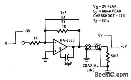
Suitable for use as radar pulse driver, video sync driver, or pulse-amplitude-modulation line driver. Uses Harris HA-2530/2535 wideband amplifier having high slew rate. Usable bandwidth is about 100 kHz when connected for noninverting operation as shown. Driver output is 60 mA into 60-ohm load. 5% settling time is 60 ns.- Linear & Data Acquisition Products, Harris Semiconductor, Melbourne, FL, Vol. 1, 1977, p 7-54 (Application Note 516). (View)
View full Circuit Diagram | Comments | Reading(1094)
LOW_COST_STROBE
Published:2009/7/14 4:22:00 Author:May
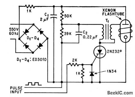
Addition of silicon controlled rectifier in triggering circuit of $20 automobile engine-timing strobe gives low-cost general-purpose stroboscope. Modification is completed by wrapping ten turns of No. 18 bare copper wire around flashtube and connecting one end to photoflash transformer T1, with other end unconnected. Can be triggered by 10-microsec 3.v pulse at 5 ma, up to 25 times per second. Flash duration is 100 microsec .-A. C. Eberle , low-Cost Strobe Built with SCR in Trigger, Electronics, 39:14, p 80-81. (View)
View full Circuit Diagram | Comments | Reading(1774)
MISSING_PULSE_DETECTOR
Published:2009/7/15 3:32:00 Author:Jessie
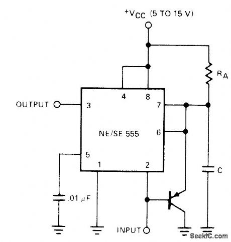
Timing cycle of 555 timer is continuously reset by input pulse train. Change in input frequency or missing pulse allows completion of timing cycle, producing change in output level. Component values should be chosen so time delay is slightly longer than normal time between pulses.- Signetics Analog Data Manual, Signetics, Sunnyvale, GA, 1977, p 723. (View)
View full Circuit Diagram | Comments | Reading(4693)
ADJUSTABLE_STROBE
Published:2009/7/14 4:21:00 Author:May
Provides time-motion data not possible with ordinary strobe. Used in studying motions where velocity varies during cycle, as in sewing machines, switches, relays, motors, and vibrating parts. Viewer can change motion point being studied by turning switch that gives choke of l00 different viewing positions.-J. H. Blakeslee, Strobe Techniques Analyze Complex Mechanical Motion, Electronics, 32:23, p 62-64. (View)
View full Circuit Diagram | Comments | Reading(810)
_12_V_AT_300_mA_FROM__48_V
Published:2009/7/14 4:20:00 Author:May
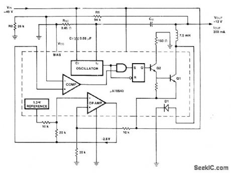
Uses Fairchild μA78S40 switching regulator having variety of internal functions that can provide differing voltage step-up, step-down, and inverter modes by appropriately connecting external components. Efficiency is 86%, and output ripple is 300 mV. Extra opamp on chip is used to derive required reference voltage of -2.6 V from internal :.3-V reference.-R. J. Apfel and D. B. Jones, Universal Switching Regulator Diversifies Power Subsystem Applications, Computer Design, March 1978, p 103-112. (View)
View full Circuit Diagram | Comments | Reading(541)
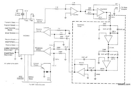
BANDPASS_ORIGINATE_FILTER
Published:2009/7/14 4:19:00 Author:May
Provides gain of over 15 dB between 1975 and 2275 Hz, to accept 2025-2225 Hz, signals of low-speed modem system using Motorola MC6860 IC,-J. M. DeLaune, “Low-Speed Modem System Design Using the MC6860,”Motorola, Phoenix, AZ、1975, AN-747, p13 (View)
View full Circuit Diagram | Comments | Reading(808)
STROBE_OSCILLAIOR_TRIGGER
Published:2009/7/14 4:19:00 Author:May
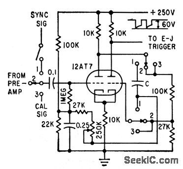
Oscillator produces square pulses having short rise time, over total frequency range of 200 to 1. Osdllator may also be sychronized to power line. Schmitt trigger provides additional means of getting output pulse to drive Eccles-Jordan trigger that provides alternate pulses for two shored-cycle strobe lamps.-L. H. Barrett, New Circuit Improves Stroboscope Versatility, Electronics, 32:32, p 116-118. (View)
View full Circuit Diagram | Comments | Reading(717)
DIGITALLY_CONTROLLED_VARIABLE_LOW_PASS
Published:2009/7/14 4:18:00 Author:May
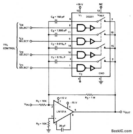
DG201 CMOS analog switch with TTL control permits setting of break frequency at 1, 10, 100, or 1000 Hz. Voltage gain below break frequency, determined by ratio of R3 to R1, is 100 (40 dB). Highest break frequency (1000 Hz) is obtained when C4 is switched in.- Analog Switches and Their Applications, Siliconix, Santa Clara, CA, 1976, p 7-66-7-67. (View)
View full Circuit Diagram | Comments | Reading(898)
ANSWER_MODEM
Published:2009/7/14 4:17:00 Author:May
Transmits on upper channel (mark 2225 Hz and space 2025 Hz) and receives on lower channel (mark 1270 Hz and space 1070 Hz). Buffer and duplexer provide modem interface to transmission network. Bandpass filter allows only desired receive signals to be seen by limiter and demodulator. Motorola MC6860 modem IC contains modulator, demodulator, and supervisory control functions. -G. Nash, Low-Speed Modem Fundamentals, Motorola, Phoenix, M, 1974, AN-731, p6. (View)
View full Circuit Diagram | Comments | Reading(856)
REMOTE_DATA_STATION
Published:2009/7/15 5:00:00 Author:Jessie
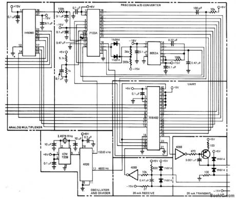
Circuit monitors DC voltages applied to pins 19 and 20 of IH5060 multiplexer and converts them to digital format for transmission as serial data to remote microprocessor. IM6100 remote host processor sends control signals to IM6402 UART to select individual multiplexer channels. Single 7209 oscillator provides clock signal for A/D converter and UART. Developed for use with Intercept Jr. microprocessor system.-S. Osgood, Remote Data Station Simplifies Data Gathering, EDN Magazine, Jan. 20, 1978, p 38 and 41. (View)
View full Circuit Diagram | Comments | Reading(1008)
TRANSISTOR_MAGNETIC_INVERTER
Published:2009/7/15 4:59:00 Author:Jessie
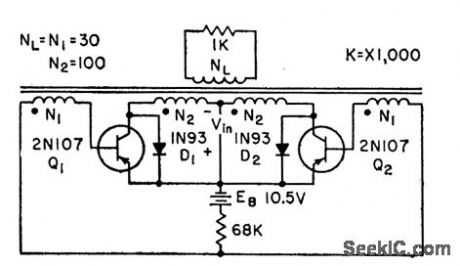
Signal conversion performance is comparable to that of electromechanical vibrator converters. For power conversion, can be substituted for dynamotor in producing high voltage from low-voltage d-c power source.-C. H. R .Campling, Magnetic Inverter Uses Tubes or Transistors, Electronics, 3:11, p 158-161. (View)
View full Circuit Diagram | Comments | Reading(821)
PULSED_DEMODULATOR
Published:2009/7/15 4:58:00 Author:Jessie
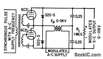
Used to provide voltage to modulating anode of klystron power amplifier at control totes above 10 cps, in system that controls output power of uhf tropospheric communications links in ac cordance with received signal at opposite end of link, to compensate for fading.-L. P.Yeh, Loop Controls Scatter Power to Offset Fading, Electronics, 32:5, p 60-62. (View)
View full Circuit Diagram | Comments | Reading(711)
LOG_ANTILOG_DIVIDER
Published:2009/7/14 4:16:00 Author:May

Can be used in applications where both numerator and denominator are restricted to single polarity (to onequadrant),Input variables X, Y andZ are applied to three indeρendent transd log amplifiers(A1- Q1A, A2- Q2A, and A3-Q2B ).Outputs of logamps are proportional to logarithms of input variables. R4, in feedback circuit of A4 converts collector current of Q1B to output voltage proportional to VZ VY / VX. Circuit performs multiplication and division simultaneously and with equal accuracy. Overall nonlinearity can be as low as 0.05%. Article gives design equations.-L.Counts and D. Sheingold, Analog Divider:WhatChoice Do You Have?, EDN Magazine, May 5, 1974, p 55-61. (View)
View full Circuit Diagram | Comments | Reading(848)
SYNCHRONOUS_DETECTOR
Published:2009/7/15 4:57:00 Author:Jessie
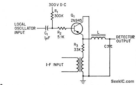
Linear deteclion permits variation of bandwidth after detection in pcm receivers. Also used us a-m detector and for measuring phase and amplitude of unmodulated signcds.-G. S. Parks, Detector Circuit Measures Phose and Amplitude, Electronics, 38:12, p 84-85. (View)
View full Circuit Diagram | Comments | Reading(1374)
TRANSISTOR_AS_SMOOTHING_FILTER
Published:2009/7/14 4:16:00 Author:May
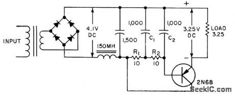
Single junction transistor in liter network of low-voltage power supply permits use of smaller fiber capacitors and chokes. Used in calibrating d-c meters up to 1 amp, at which residual peak-to-peak ripple values are 0.0015 amp and 0.005 v.-F. Oakes and E. W. Lawson, Transistor Filters Ripple, Electronics, 31:15, p 95. (View)
View full Circuit Diagram | Comments | Reading(942)
45_30_V_SWITCHING_AT_6_A
Published:2009/7/14 4:14:00 Author:May
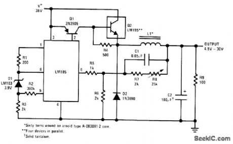
LM105 positive regulator serves as amplifier-reference for LM195 power transistor IC in switching regulator. Duty cycle of switching action adjusts automatically to give constant output. Q2 consists of four LM195s in parallel since each is rated at only about 2 A. R8 serves as output voltage control- Linear Applications, Vol. 2, National Semiconductor, Santa Clara, CA, 1976, AN-110, 3.9V p4. (View)
View full Circuit Diagram | Comments | Reading(1358)
GENERAL_FILTER
Published:2009/7/14 4:14:00 Author:May
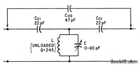
Bridging conventional bandpass filter with single capacitor C00 converts to general fiber having both sharp pass and reject behavior at adjacent frequencies. For values shown, bandpass occurs at 20 Mc and peak rejection frequency is 19.15 Mc.-R. Kurzrok, Single Component Changes Bandpass into General Filter, Electronics, 39:8, p 95-96. (View)
View full Circuit Diagram | Comments | Reading(875)
| Pages:148/471 At 20141142143144145146147148149150151152153154155156157158159160Under 20 |
Circuit Categories
power supply circuit
Amplifier Circuit
Basic Circuit
LED and Light Circuit
Sensor Circuit
Signal Processing
Electrical Equipment Circuit
Control Circuit
Remote Control Circuit
A/D-D/A Converter Circuit
Audio Circuit
Measuring and Test Circuit
Communication Circuit
Computer-Related Circuit
555 Circuit
Automotive Circuit
Repairing Circuit