
Basic Circuit
Index 149
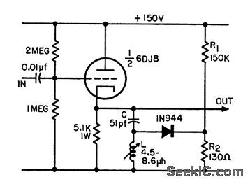
TRANSISTORIZED_MAGNETOSTRICTION_BAND_PASS_FILTER
Published:2009/7/14 4:14:00 Author:May
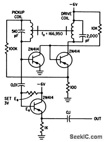
Three transistors and filter give stable fixed-frequency oscillator, with over all gain of 20 db and maximum linear out-put of 1 v rms.-E. J. Neville, Jr., Designing Magnetostriction Filters, Electronics, 33:51, p 88-89. (View)
View full Circuit Diagram | Comments | Reading(1034)
PARALLEL_INVERTER_FOR_REACTIVE_LOADS
Published:2009/7/15 4:55:00 Author:Jessie
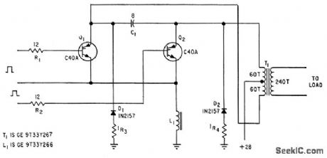
Produces square-rave output under all load conditions, without creating high voltages across silicon controlled rectifiers during light loads.-D. V. Jones, Turn-Off Circuits for Controlled Rectifiers, Electronics, 33:32, p 52-55. (View)
View full Circuit Diagram | Comments | Reading(712)
CASCADED_HIGH_AND_LOW_PASS_A_F
Published:2009/7/14 4:13:00 Author:May
Slope can be any desired multiple of 12 db per octave, with insertion loss less than 2 db.Corner frequencies are 200 radians per sec (32 cps) and 40,000 radians per sec (6,370 cps).-W. D. Fryer, How to Design Low Cost Audio Fillers, Electronics, 32:15, p 68-70. (View)
View full Circuit Diagram | Comments | Reading(823)
WIEN_BRIDGE_FILTER
Published:2009/7/14 4:13:00 Author:May
Does not have high Q but provides good rejection (40 db attenuation with 1 % tolerance components and 60 db with 0.1% tolerance components).-J. K. Goodwin, Wien Bridge Forms Rejection Filter, Electronics, 32:1, p 58-59. (View)
View full Circuit Diagram | Comments | Reading(0)
DYNAMIC_NOTCH_FILTER
Published:2009/7/14 4:12:00 Author:May
Will trap out 10-Mc noise while passing 10.Mc signal in heterodyne frequency convertor used to extend measurement range of 10-Mc counter. Operation is based on difference in level of noise and desired signal. Dynamic action of filter nulls out low-level noise, but filter disappears in presence of desired high-level signal. -H. T. McAleer, Dynamic Notch Filter, FEE, 10:9, p 90-91. (View)
View full Circuit Diagram | Comments | Reading(931)
LATTICE_COUPLING_OF_DOUBLE_TUNED_FILTER
Published:2009/7/14 4:11:00 Author:May
Permits adjusting coupling between input and output resonant circuits to com pensate for stray reactances and variations in component values. Used in 30.Mc i-f amplifier requiring 1-Mc bandwidth. One side of variable capacitor is grounded, per mitting convenient mechanical design.-J. H. Grindon, Lattice Coupling of Resonant Circuits, EEE, 13:6, p 53-55. (View)
View full Circuit Diagram | Comments | Reading(746)
100_mA_CURRENT_REGULATOR
Published:2009/7/14 4:11:00 Author:May
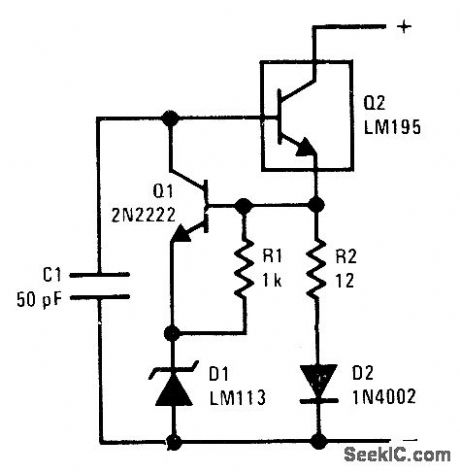
Two-terminal circuit using LM195 power transistor has low temperature coefficient and operates down to 3 V. 2N2222 controls voltage across current-sensing resistor R2 and diode D1. Voltage across sense network is base-emitter voltage of 2N2222 plus 1.2 V from LM113. R1 sets current through LM113 to 0.6 mA. -R. Dobkin, Fast IC Power Transistor with Thermal Protection, National Semiconductor, Santa Clara, CA, 1974. AN-110, p6. (View)
View full Circuit Diagram | Comments | Reading(0)
PSEUDORANDOM_CMOS
Published:2009/7/15 4:53:00 Author:Jessie
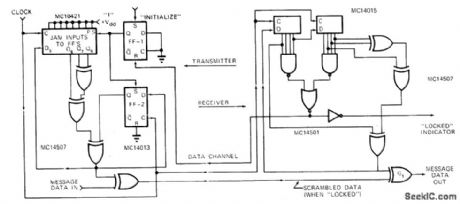
Uses MC14021 8-bit shift register in conjunction with MC14507 EXCLUSIVE-OR gates to generate pseudorandom digital code. To develop code pattern, 1st, 6th, 7th, and 8th bits are sent through EXCLU-SIVE-OR gates and fed back to shift-register input. Output can be used as random test signal or for protecting messages sent over public channels or stored in public files. Digital message is scrambled by mixing it with output of code generator in EXCLUSIVE-OR gate. Functionally identical 255-bit random generator is used at receiver to unscramble data. Decoding circuit must have access to sending clock and means for synchronizing so as to put both registers into all-1 state. Register in receiver goes through all its states within 255 clock pulses; when it reaches all-1 state, signal is fed back to sender for releasing FF-1 so scrambling can commence. Article traces operation in detail. -J. Halligan, Pseudo-Random Number Generator Uses CMOS Logic, EDN Magazine, Aug. 15, 1972, p 42-43. (View)
View full Circuit Diagram | Comments | Reading(1499)
TWIN_T_400_CPS_FILTER
Published:2009/7/14 4:11:00 Author:May
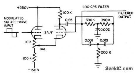
Used with modulators lo increase signed-noise ratio. Filter is tuned to 400 cps, and eliminates other frequencies by feeding them back. Q of fiber is 6. Output is low-distortion sine wave in phase with input. Frequency regulation of cattier signal should be barter than 1% or liter will introduce phase shift.-L. S. Klivans, Modulators for Automatic Control Systems, Electronics, 31:1, p 82-84. (View)
View full Circuit Diagram | Comments | Reading(905)
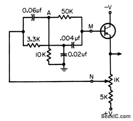
CONTROL_CIRCUIT_CUTS_INVERTER_IDLINGCURRENT
Published:2009/7/15 4:52:00 Author:Jessie
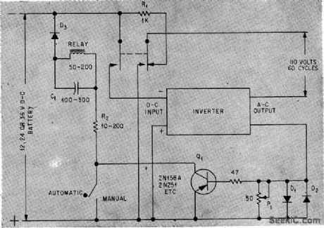
Reduces standby current to less than1 ma. Sensing element is pair of back- to-back silicon diodes, D1 and D2. Used when a-c power must be available on demand at many remote outlets even though actually ; used only few hours a day.-D. W. R. McKinley, Inverter Control Circuit Saves Power, Electronics, 34:31, p 56. (View)
View full Circuit Diagram | Comments | Reading(791)
WIRED_OR_TERMINALS
Published:2009/7/15 4:50:00 Author:Jessie
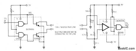
Arrangement permits connecting several IC line drivers in parallel for feeding single 100-ohm twisted-pair data line. With wired-OR transmitting capability, TTL output of receiver at right is logic 1 only if all paralleled drivers are transmitting logic 1. If any one or all of drivers transmit logic 0, output of receiver logic 0,-D, Pippenger, Termination Is the Key to Wired-OR Capability, EDN/EEE Magazine, Dec 15, 1971, p17. (View)
View full Circuit Diagram | Comments | Reading(773)
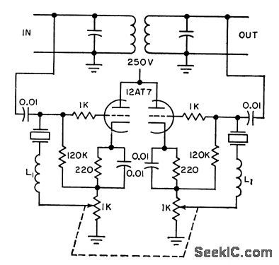
ACTIVE_800_CPS_PARALLEL_T_FILTER
Published:2009/7/14 4:10:00 Author:May
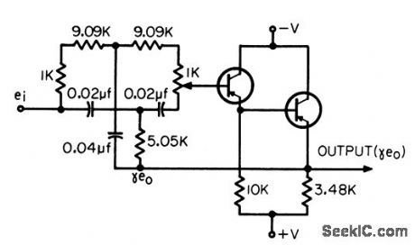
Potentiometer adjusts amount of rejection to compensate for tolerances of components. Second emitter-follower provides lower output impedance so feedback to network is more effective in sharpening notch of filter characteristic and in decreasing phase shift around null frequency. Used in servo sys terns.-T. Mollinga, Actiye Parallel-T Net.works, EEE, 14:4, p 93-98, (View)
View full Circuit Diagram | Comments | Reading(923)
DUAL_DETECTORS_PREVENT_LOCKING_ON_SIDEBANDS
Published:2009/7/15 4:49:00 Author:Jessie
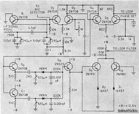
Antisideband circuit rejects side-band locking while telemetry tracking loop is automatically searching for signals around i-f value. Circuit also provides both p-m and aim demodulation. Emitter-follower Q1, receiving i-f signal, feeds discriminator Q6-07 through limiters Q2-Q3 and Q4-05. For 455-kc input, d-c outputs of diode detectors cancel at hose of Q8. For lower or higher frequencies, difference voltage serves to apply antisideband error signal to loop fiber through Q9 or Q10.-W. H. Casson and C. C. Hall, New Phase-Tracking Demodulator Will Not Lock on Sidebands, Electronics, 36:6, p 52-55. (View)
View full Circuit Diagram | Comments | Reading(723)
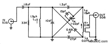
TRIPLE_TUNED_90_OHM_INPUT
Published:2009/7/14 4:10:00 Author:May
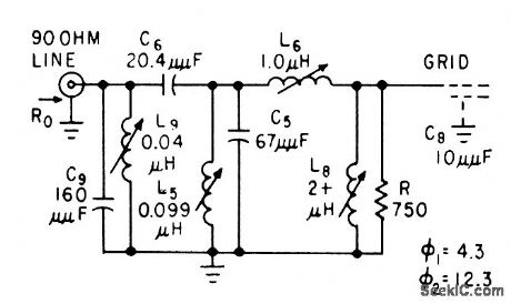
Article gives design procedure. Example shown passes signals between 55 and 65.5 Mc.-R. B.Hirsch, How to Design Bandpass Triples, Electronics, 32:34, p 41-44. (View)
View full Circuit Diagram | Comments | Reading(772)
PROGBAMMED__DIVIDE_BY_179
Published:2009/7/14 4:09:00 Author:May
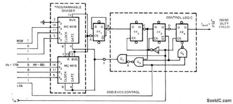
Produces symmetrical output waveforms even if divider ratios are large, variable, and even or odd. Circuit is set up for output of N = 179, for which M= 89 is programmed into divider and odd/even control of logic is a .0 Control logic can be simplified, depending on particular requirements; thus, if perfect symmetry is notessential,G4 and FF4 can be eliminated, Article tells how to program for any other value of N.-V. R. Godbole, Programmable Divider Maintains Output Symmetry, EDN Magazine, July 5, 1974, p 72-74.
(View)
View full Circuit Diagram | Comments | Reading(723)
16_30_MHz_20_W_LINEAR_DRIVER
Published:2009/7/14 4:09:00 Author:May

Broadband amplifier using inexpensive plastic RF power transistors provides total power gain of about 25 dB for driving SSB transmitter power amplifiers to levels up to several hundred watts. Supply is 13.6 V. Circuit is stable even with load mismatches of 10:1.-H. 0. Granberg, Low-Distortion 1.6 to 30 MHz SSB Driver Designs, Motorola, Phoenix, AZ, 1977, AN-779, p 3.
(View)
View full Circuit Diagram | Comments | Reading(821)
VARIABLE_BANDWIDTH_848_KC_CRYSIAL_FILTER
Published:2009/7/14 4:09:00 Author:May
High-Q unbalanced crystal filter is easy to adjust over appreciable frequency range,Can be used in f-m oscillators, signal generators, and i-f amplifiers, as well as in variable-bandwidth filters.-J. C. Seddon, Stable Crystal Filter is Parallel Resonant, Electronics, 31:11, p 155-156. (View)
View full Circuit Diagram | Comments | Reading(775)
BANDPASS_ANSWER_FILTER
Published:2009/7/15 4:47:00 Author:Jessie

Provides gain of 15 dB over bandwidth of 1020 to 1320 Hz for low-speed modem system using Motorola MC6860 IC. Attenuation is 35 dB at 2225 Hz, as required for answer-only modem system. Equations for values of filter components are given.-J. M. DeLaune, Low-Speed Modem System Design Using the MC6860, Motorola, Phoenix, AZ, 1975, AN-747, p 10. (View)
View full Circuit Diagram | Comments | Reading(697)
800_CPS_OSCILLATOR_WITH_PARALLEL_T_FILTER
Published:2009/7/14 4:08:00 Author:May
R-C network in feedback loop determimes frequency of oscillation.-T. Mollinga, Active parallel-T Networks, EEE, 14:4, p 93-98. (View)
View full Circuit Diagram | Comments | Reading(766)
MONO_PULSE_SHRINKER
Published:2009/7/15 4:45:00 Author:Jessie
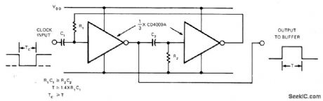
Duty cycle of clock pulse is shortened by two CMOS inverters used to form negative-transition triggered mono-stable multivibrator. Duration of output pulse T is about 1.4R1C1. Output pulse occurs each time input clock goes from high to low. Used with foldback current limiting for short-circuit protection in clock-driven regulated power supply. Low duty cycle of dock pulses ensures positive full-load starting of supply.-J. L. Bohan, Clocking Scheme Improves Power Supply Short-Circuit Protection, EDN Magazine, March 5, 1974, p 49-52. (View)
View full Circuit Diagram | Comments | Reading(1368)
| Pages:149/471 At 20141142143144145146147148149150151152153154155156157158159160Under 20 |
Circuit Categories
power supply circuit
Amplifier Circuit
Basic Circuit
LED and Light Circuit
Sensor Circuit
Signal Processing
Electrical Equipment Circuit
Control Circuit
Remote Control Circuit
A/D-D/A Converter Circuit
Audio Circuit
Measuring and Test Circuit
Communication Circuit
Computer-Related Circuit
555 Circuit
Automotive Circuit
Repairing Circuit