
Basic Circuit
Index 152
BUS_TRANSCEIVER
Published:2009/7/15 4:17:00 Author:Jessie
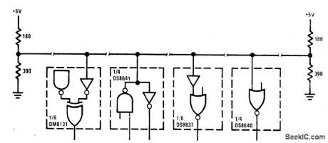
Designed for use in bus-organized data transmission systems interconnected by terminated 120-ohm lines. Up to 27 driver/receiver pairs can be connected to common bus. One two-input NOR gate is included in National DS8641 quad unified bus transceiver package to disable all drivers in package simultaneously.- Interface Integrated Circuits, National Semiconductor, Santa Clara,CA, 1975, p3-17-3-18. (View)
View full Circuit Diagram | Comments | Reading(833)
PULSE_COUNTER
Published:2009/7/14 3:53:00 Author:May
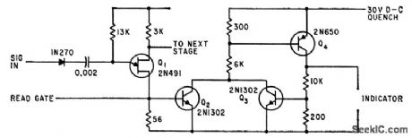
Unijunction transistor Q1 servos as counter, with other counter stages being identical. Q3 and Q4 energize and lock readout circuit until quench pulse is applied after next counting cycle.-F. W. Kear, Unijuncfion Transistor Pulse-Circuit Design, Electronics, 35:21, p 58-60. (View)
View full Circuit Diagram | Comments | Reading(1022)
_12_V_AND__15_V_FROM_4_24_V
Published:2009/7/14 3:53:00 Author:May
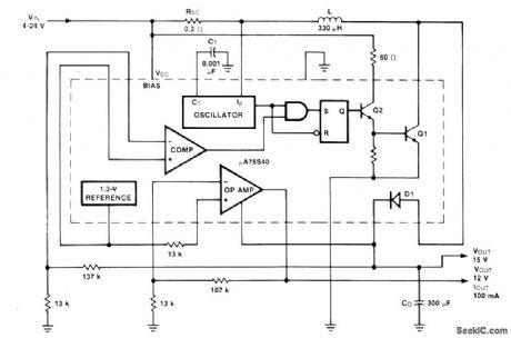
Connections shown for Fairchild μA78S40 switching regulator give universal regulator providing either step-up or step-down, for loads up to 100 mA. Efficiency is about 50% for input extremes of 4 and 24 V, increasing to maximum of 75% for other input voltages. Output ripple is essentially eliminated at 12-V output.-R. J. Apfel and D. B. Jones, Universal Switching Regulator Diversifies Power Subsystem Applications, Computer Design, March 1978, p 103-112. (View)
View full Circuit Diagram | Comments | Reading(499)
BLACK_LIGHT_INVERTER
Published:2009/7/15 4:14:00 Author:Jessie
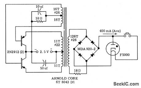
Operates from 2.5-v rechargeable battery and supplies 400 ma at 26 v to gas arc tube for portable ultraviolet lamp. Efficiency is 80%.-H. F. Weber, Low Voltage Inverter Features High Frequency Operation with High Efficiency, Motorola Application Note AN-174, Feb. (View)
View full Circuit Diagram | Comments | Reading(1129)
AUTOMATIC_THRESHOLD_CONTROL_REJECTS_NOISE
Published:2009/7/14 3:52:00 Author:May
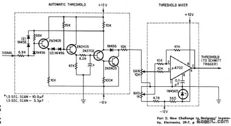
Provides varying threshold control voltage that causes detection threshold of celestial guidance system to operate at level slightly above background noise. After clipping by amplifier, signal enters threshold-shaping unit that operates as fastrise, slow-fall agc.- R. L. Lillestrand, J. E. Carroll, and J. S. Newcomb, Automatic Celestial Guidance, Part 2: New Challenge to Designers' Ingenuity, Electronics, 39:7, p 94-105. (View)
View full Circuit Diagram | Comments | Reading(688)
SYNC_CIRCUIT_FOR_QUINARY_SCALER
Published:2009/7/14 3:52:00 Author:May
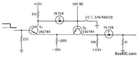
Time-base signal at 500 Mc turns Q1 on and Q2 off at timing rate. Negative 1-V start signal applied to base of Q1 makes 500-Mc signal appear at collector of Q2 to serve as output for one of quinary scalers. Two scalers in parallel can measure time accurately to within 1 nsec. -R. Englemann, Quinary Scalers: Measure time Intervals Digitally, Electronics, 37:5, p 34-36. (View)
View full Circuit Diagram | Comments | Reading(720)
3_KILOBAUD_FULL_DUPLEX_FSK_MODEM
Published:2009/7/15 4:14:00 Author:Jessie
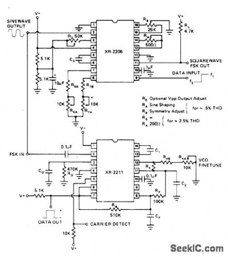
Values shown are for 13-kHz bandwidth、1070 Hz for mark and 1270 Hz for space, using Exar XR-2206 function generator and XR-2211 FSK de-modulator Report gives design procedure,Supply can be +12 v.- Phase-Locked Loop Data Book, Exar Integrated Systems, Sunnyvale, CA, 1978, p 57-61. (View)
View full Circuit Diagram | Comments | Reading(4864)
SIMPLE_LED_THERMOMETER
Published:2009/7/14 3:50:00 Author:May

As shown, the circuit is powered by a 9-V battery, B1, but it can easily run off any 7- to 10-Vdc power supply. At the heart of the thermometer is IC1, an LM34 temperature sensor. That device produces a voltage between the Vout and GND terminals that is linearly proportional to temperature. Al-though the output is usually 10 mV/°F, IC1 is connected in a resistor network (made up of R1 to R3) with a gain that provides an output of 40 mV/'°F Capacitor C1 is used as a noise bypass across R1 and R2. Because the voltage output by IC1 will be used by the rest of the circuit to determine what the temperature in the room is, potentiometer R1 will have to be calibrated exactly. The output of IC1 is fed to pin 5 of IC2, an LM3914 LED bar- or dot-graph driver, which is where the actual temperature-determining process occurs. IC2 has 10 internal comparators, the output pins of which are connected to LED1 to LED10. The voltage input to pin 5 is compared by IC2 to the voltages at pins 4 and 6; that process determines which LED or LEDs light. The LEDs can be set to light either one at a time (dot mode) or progressively (bar mode). When jumper JU1 is not installed, dot mode is enabled.When the jumper is installed, the chip is in bar mode. In dot mode, the LED that corresponds to the correct input voltage lights by itself. When the input voltage increases, an LED representing a higher temperature will light and the LED previously lit will extinguish. In bar mode, the LED representing the temperature will light and all of the lower LEDs will stay lit. Each mode has its advantages-the dot mode uses less current because only one LED is lit at a time, but the bar mode is easier to read at a glance. Resistor R8 and capacitor C2 provide decoupling for the LED-supply circuit. If bar-mode operation is desired, it is recommended that you reduce the value of R8 to 15Ω For a range of 60 to 78°F to be displayed, pin 6 must have a reference of 3.345 V and pin 4 should have a reference of 2.545 V. Those values are obtained through adjustments of potentiometers R5 and R7. (View)
View full Circuit Diagram | Comments | Reading(2517)
EXCLUSIVE_OR_GATES
Published:2009/7/15 4:12:00 Author:Jessie
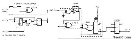
Use of retriggerable mono with EXCLUSIVE-OR gates simplifies design of both transmitter and receiver for handling binary phase-modulated digital data over single line.With 50% duty-cycle clock at transmitter, clock and data signals are applied to Inputs of 9014 to generate output signal for line. At receiver, clock and data stream are regenerated by 9601 adjusted to 75% of data-bit time and connected in nonretriggerable mode. One EXCLUSIVE-OR gate and an EXCLUSIVE-NOR gate connected as inverting delay element will trigger 9601. System remains synchronized as long as pulse width of mono is between 50% and 100% of data-bit time. -P. Alfke, Exclusive-OR Gates Simplify Modem Designs, EDN Magazine, Sept. 15, 1972, p 43. (View)
View full Circuit Diagram | Comments | Reading(1339)
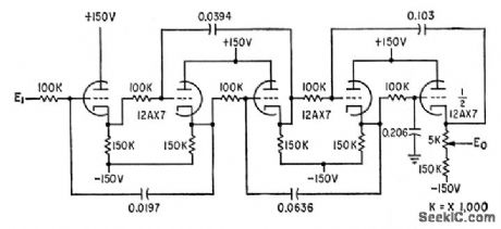
TUNED_A_F
Published:2009/7/14 3:49:00 Author:May
R2 tunes three-step ladder net-work of feedback loop from 800 to 1,000 cps. Circuit is stable. Used in a-c bridge.-J. F. Delpech, SimpleCircuit Tunes Audio Amplifier, Electronics, 38:6, p 84-85. (View)
View full Circuit Diagram | Comments | Reading(769)
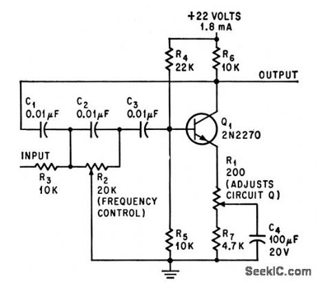
CURRENT_SOURCE_AS_TRANSISTOR_LOAD
Published:2009/7/14 3:49:00 Author:May


Reverse-biased germanium diode serves as voltage-independent current source for loading silicon transistors in linear amplifier having voltage gain of 50 and -3 dB bandwidth of t6-4000 Hz. In addition to low cost, circuit design permits reliable operation of reliable micro-power circuits over wide temperature range at optimum current drain. -M. G. Baker, Low-Cur-rent Source, Wireless World, April 1976, p 61. (View)
View full Circuit Diagram | Comments | Reading(1575)
LOW_VOLTAGE_HIGH_CURRENT_INVERTER
Published:2009/7/15 4:10:00 Author:Jessie
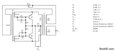
Converts output of solar cells, fuel cells, and other low-voltage sources to higher voltage sources. Currents up to 50 amp can be switched efficiently by 2N2728 power transistors used. Circuit shown provides ac output which can easily be changed to d-c at desired higher voltage by rectifying and filtering Use of two transformers minimizes core losses when switching high collector currents. Efficiency is 70% at 60 w output. -J. Takesuye, “A Low Voltage High Current Converter.” Motorola Application Note AN-169. Dec, 1965. (View)
View full Circuit Diagram | Comments | Reading(951)
PHONOTAPEAND_MICROPHONE_PREAMP
Published:2009/7/14 3:58:00 Author:May
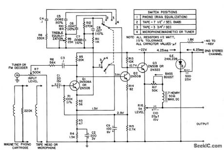
Total harmonic or intermodulation distortion isless than 0.3% at reference level output of 1 v. Will take most magnetic pickupimpedances. Equalized output is constant within 1 db from 40 cps to 12 kc. - Transistor Manual , Seventh Edition ,General Electric Co.,1964,p 252. (View)
View full Circuit Diagram | Comments | Reading(873)
FET_AMPLIFIER_FOR_ACTIVE_FILTER
Published:2009/7/14 3:57:00 Author:May
Meets gain stability and high input impedance requirements for use with third-order lowpass active filters. Uses bootstrapped source-follower. Drain of input fet drives pnp transistor in cascode to reduce input capacitance.-L. J. Sevin, Jr., Field-Effect Transistors, McGraw-Hill, N.Y., 1965, p 105. (View)
View full Circuit Diagram | Comments | Reading(994)
6_V_FOR_CALCULATOR
Published:2009/7/14 3:57:00 Author:May
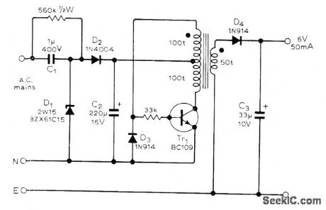
Can be mounted in housing of calculator or small transistor radio, for operation from AC line. D1 and D2 produce 15 VDC across filter capacitor C2 as supply for inverter Tr1 operating at 13 kHz. Transformer is wound with No. 37 wire on small core such as Phillips P14/8 337 pot core. Primary windings are bifilar. Use grounded shield to reduce radiated switching noise.-M. Faulkner, Miniature Switch Mode Power Supply, Wireless World, Oct. 1977, p 65. (View)
View full Circuit Diagram | Comments | Reading(795)
ZOBEL_BAND_PASS_FILTER
Published:2009/7/14 3:57:00 Author:May

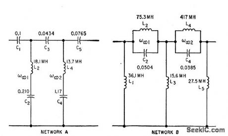
Both examples give at least 40 db attenuation below 7,500 cps and above 12,500 cps, for 600-ohm source and load resistances.-K.Lichtenfeld, Method for Simplifying Filler Design, Electronics, 33:2, p 96-99. (View)
View full Circuit Diagram | Comments | Reading(899)
ACTIVE_BUTTERWORTH_R_C_FILTER
Published:2009/7/14 3:56:00 Author:May
Article gives design procedure for selecting R and C values for active filters characterized by zero output either at zero frequency or at in infinite frequency. Symmetry of network transfer function allows choice of values by coefficient matching technique. Fifth-order low-pass filter, down 50 db at 70 cps, is shown.-R. E. Bach, Jr., Selecting R-C Values for Active Filters, Electronics, 33:20, p 82-85. (View)
View full Circuit Diagram | Comments | Reading(841)
PROGRAMMED_0_255_V
Published:2009/7/14 3:56:00 Author:May
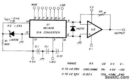
Uses D/A converter and 2.5-V zener to form digitally programmed voltage reference. Binary-coded TTL information selects voltage ranges of 0-2.55 V or 0-25.5 V. Can be used as lab source having 10 mV per step in low range and 100 mV per step in high range. Output is adjusted with 8-bit input control. R3 determines basic voltage range, being set at 1280 ohms for low range and 12.8K for high range, Although 741 or other general-purpose opamp is adequate for low range, higher-voltage single-supply opamp such as 759 is better for high range and for both ranges, because it gives higher output current on low range.-W. Jung, An IC Op Amp Update, Ham Radio, March 1978, p 62-69. (View)
View full Circuit Diagram | Comments | Reading(727)
ELECTRONIC_FADER
Published:2009/7/14 3:55:00 Author:May
used to fade audio signals on and off without Producing audible switching transients. signals from matching network of driver are applied to Point A and B.-E. de Boer Electronic Fader for Auditory Research,Electronics,33:50,p 85-87. (View)
View full Circuit Diagram | Comments | Reading(810)
HIGH_VOLTAGENE_GATIVE_SWIT_CHING
Published:2009/7/14 3:55:00 Author:May
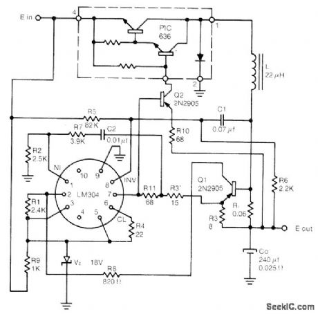
Designed for operation from supply voltages above maximum of -40 V for LM304 regulator, Output is -5 V at up to 10 A. Q2 provides volt-age isolation between regulator and Unitrode PIC636 hybrid power switch. R9 limits current through zener under steady-state and start-up conditions.- Switching Regulator Design Guide, Unitrode, Watertown, MA, 1974, U-68A, p 9. (View)
View full Circuit Diagram | Comments | Reading(731)
| Pages:152/471 At 20141142143144145146147148149150151152153154155156157158159160Under 20 |
Circuit Categories
power supply circuit
Amplifier Circuit
Basic Circuit
LED and Light Circuit
Sensor Circuit
Signal Processing
Electrical Equipment Circuit
Control Circuit
Remote Control Circuit
A/D-D/A Converter Circuit
Audio Circuit
Measuring and Test Circuit
Communication Circuit
Computer-Related Circuit
555 Circuit
Automotive Circuit
Repairing Circuit