
Communication Circuit
Index 14
SIGNAL_POWERED_ALARM_RECEIVER
Published:2009/7/10 1:25:00 Author:May
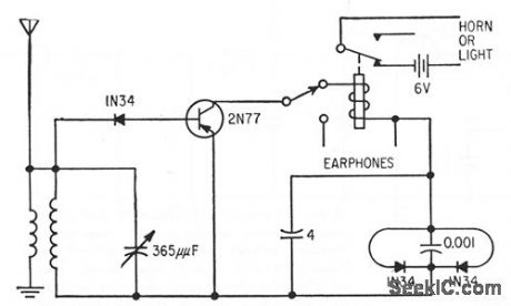
On arrival of carrier signal at frequency to which antenna and input are tuned, transistor pulls in relay applying battery power to horn or light. No power is drawn front battery during standby time. For signals below 50 Mc,best pick up is obtained with single-wire an tenna 150 feet long, at right angles to line.of-sight path and as high as possible.-L.R.Crump, Radio Waves Power Transistor Circulls, Electron'Ics, 31:19, p 63-65. (View)
View full Circuit Diagram | Comments | Reading(1122)
FERRITE_BEAD_CURRENT_TRANSFORMER
Published:2009/7/9 23:01:00 Author:May
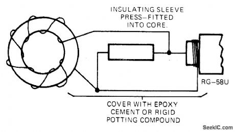
No. 27 ferrite bead (Ferronics 11-122-B) wound with 25 turns No. 30 enameled wire and shunted by 50-ohm1/4-W resistor, gives low-cost transformer that can be used in range of 3 kHz to 30 MHz. Current-conversion ratio is 1 V/A into 50-ohm coaxial-cable termination, with excellent linearity from milliamperes up into amperes. Wire carrying current to be measured is passed once through core, to serve as singleturn primary of transformer.-M. Salvati, Ferrite Bead Makes Cheap Current Transformer, EDN Magazine, March 20, 1974, p 85. (View)
View full Circuit Diagram | Comments | Reading(2345)
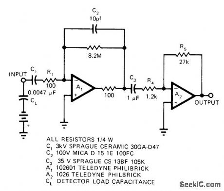
PRECISION_FULL_WAVE_RECTIFIER
Published:2009/7/9 22:37:00 Author:May
This circuit provides accurate full-wave rectification. The output impedance is low for both input polarities, and the errors are small at all signal levels. Note that the output will not sink heavy currents, except a small amount through the 10-KΩ resistors. Therefore, the load applied should be referenced to ground or a negative voltage. The reversal of all diode polarities will reverse the polarity of the output. Since the outputs of the amplifiers must slew through two diode drops when the input polarity changes, the 741-type devices give 5% distortion at about 300 Hz. (View)
View full Circuit Diagram | Comments | Reading(2346)
DIGITAL_DATA_LINE_RECEIVER__
Published:2009/7/9 22:29:00 Author:May

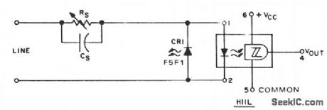
When digital data is transmitted over long lines (longer than 1 meter), proper transfer is often disturbed by the parasitic effects of ground level shifts and ground loops, as well as by extraneous noise picked up along the way. An optocoupler, such as the H11L, combining galvanic isolation to minimize ground loop currents and their concomitant common-mode voltages, with predictable switching levels to enhance noise immunity, can significantly reduce erratic behavior. Resistor RS is programmed for the desired switching threshold, CS is an optional speed-up capacitor, and CR1 is an LED used as a simple diode to provide perfect line balance and a discharge path for CS if the speed-up capacitor is used. (View)
View full Circuit Diagram | Comments | Reading(1288)
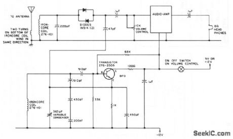
SIMPLE_HAM_BAND_RECEIVER
Published:2009/7/9 22:26:00 Author:May

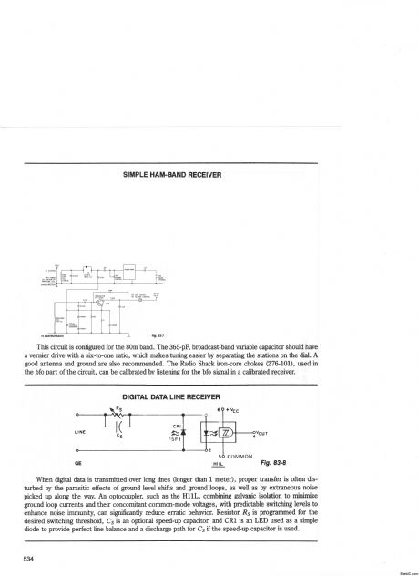
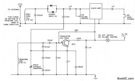
This circuit is configured for the 80m band. The 365-pF, broadcast-band variable capacitor should have a vernier drive with a six-to-one ratio, which makes tuning easier by separating the stations on the dial. A good antenna and ground are also recommended. The Radio Shack iron-core chokes (276-101), used in the bfo part of the circuit, can be calibrated by listening for the bfo signal in a calibrated receiver.
(View)
View full Circuit Diagram | Comments | Reading(1723)
FSK_DATA_RECEIVER
Published:2009/7/9 22:24:00 Author:May
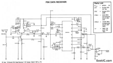
The various signal frequencies are obtained for an incoming carrier centered at 49.86 MHz. The receiver employs double conversion, with i-fs at 10.7 MHz and 455 kHz. Ceramic filters are used in both i-fs for selectivity and reduced-coil count. A quadrature detector is used to recover the baseband data, and an integrator and Schmitt trigger are used to filter the demodulated output.Also included is a squelch curcutt that functions as a status line, and the open-collector output switches high when a sianaHs received. The LM3361A functions as the 2nd LO, 2nd mixer, limiting i-f, quadrature detector, and squelch; yet, it consumes less than 4 mA from a 5-V logic supply. The entire receiver requires approximately 10 mA. (View)
View full Circuit Diagram | Comments | Reading(1394)
LOGIC_LEVEL_TRANSLATORS
Published:2009/7/9 22:23:00 Author:May
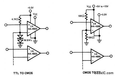
The HA-4900 senes comparators can be used as versatile logic interface devices,as shown in these circuits.Negative logic devices can also be interfaced with appropriate supply connections.If separatesupplies are used for V-and VLOGIC-,these logic-level translators will tolerate several volts of groundline differential noise. (View)
View full Circuit Diagram | Comments | Reading(1094)
LOW_COST_LINE_RECEIVER
Published:2009/7/9 22:21:00 Author:May
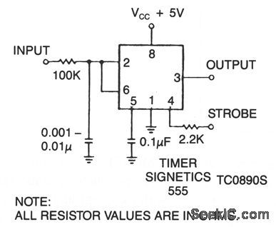
This timer makes an excellent line receiver for control applications involving relatively slow electromechanical devices. It can work without special drivers over single, unshielded lines. (View)
View full Circuit Diagram | Comments | Reading(1123)
CARRIER_CURRENT_RECEIVER_FOR_DATA_TRANSMISSION
Published:2009/7/9 22:12:00 Author:May
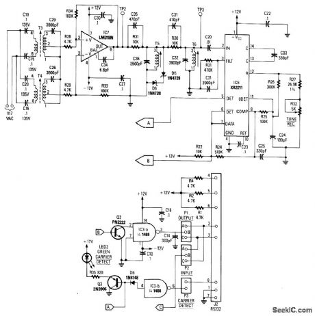
This receiver consists of an input network amplifier IC7 FSK PLL detector ICG, and output amplifier/ interface Q2, Q3, IC3A and IC3B, a 1488 Quad RS232 line driver of the carrier-current signal. Tuned amplifier IC7 amplifies this signal and drives PLL detector IC8. The values shown in the circuit are suitable for operation in the 100-kHz range. Recovered data at pins 5, 6, 7 is fed to the output amplifter/interface circuit (Fig, 6). This circuit is also used with the carrier-current data transmitter to form a pair. (View)
View full Circuit Diagram | Comments | Reading(1990)
CARRIER_CURRENT_TRANSMITTER_FOR_DATA_TRANSMISSION
Published:2009/7/9 22:09:00 Author:May


In this circuit, data at input C is amplified by IC2 and then fed to modulator IC1. IC1 generates two frequencies, depending on the values of C5, RIO, R3, R11, and R6. The frequency f, is generated if pin 9 IC1 is low and f2 if pin9lC1 is high. A square wave appears at pin 13 of IC1 and is fed to Q1, an amplifier stage, that is coupled via tuned transformer T, to the ac line via C1 and C2. Notice that, for safety reasons, C1 and C2 must be specifically rated for the ac line voltage. (View)
View full Circuit Diagram | Comments | Reading(1024)
VOLICE_MODULATED_PULSE_FM_IR_TRANSMITTER
Published:2009/7/9 21:04:00 Author:May
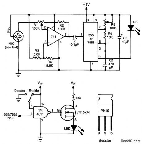
This circuit has a 741 audio amplifier, which is fed by a microphone (use an amplified type), an FM modulator, and a CMOS timer that acts as a VCO. The LED is pulsed with the timer output (the booster circuit can be used for increased range). This yields an FM-modulated, pulsed IR beam. (View)
View full Circuit Diagram | Comments | Reading(2718)
IR_TRANSMITTER
Published:2009/7/9 20:53:00 Author:May
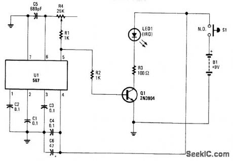
Using an NE567 as a tone oscillator, this circuit produces an IR signal from the LED, which is modu-lated with a square wave. LED1 is an IR-emitting LED. The modulation helps improve performance under high ambient light conditions. (View)
View full Circuit Diagram | Comments | Reading(0)
SIMPLE_IR_TRANSMITTER
Published:2009/7/9 20:50:00 Author:May
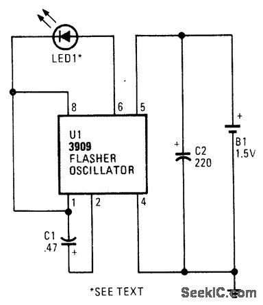
The IR diode's flash rate is determined by the value of C1, a 220-μF capacitor that sets the rate of oscillation at 1 Hz per second. Reducing C1 will increase the frequency of the circuit, while larger values will decrease the frequency.
Because the circuit only sends out single, nar-row pulses of invisible light, the IR receiver only responds with a click for every output pulse. (View)
View full Circuit Diagram | Comments | Reading(1037)
HAND_HELD_TRANSCEIVER_DCADAPTER
Published:2009/7/9 2:41:00 Author:May
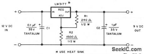
This dc adapter provides a regulated 9-V source for operating a Kenwood TR-2500 hand-held transceiver in the car. The LM317T's mounting tab is electrically connected to its output pin, so take this into account as you construct your version of the adapter. The LM317T regulator dissipates 2 or 3 W in this application, so mount it on a 1- x -2-inch piece of 1/8-inch-thick aluminum heatsink. (View)
View full Circuit Diagram | Comments | Reading(2084)
ULTRASONIC_RECEIVER
Published:2009/7/9 1:02:00 Author:May
The piezo speaker, MIC1, picks up the incoming ultrasonic signal and feeds it to the base of Q1. The two-transistor booster amplifier, Q1 and Q2, raises the signal to a level that is sufficient to drive one input of this most unusual mixer circuit.Integrated circuit U2, a quad bilateral switch, functions as an extremely clean balanced-mixer circuit for the superheterodyne receiver. Integrated circuit Ula, 1/2 of a dual op amp, is connected in a variablefrequency square-wave oscillator circuit. Resistors R5, R6, and capacitor C4 determine the frequency and tuning range of the oscillator.The oscillator's square-wave output is fed along two paths. In one path, the output of U1a is input to pins 12 and 13 of U2. In the other path, the signal is fed to the base of Q3, which is configured as an inverter. The inverter outputs a signal that is 180°out-of-phase with the input signal. The inverted output of Q3 is then fed to U2 at pins 5 and 6. There, the two input signals, the ultrasonic input from MIC1 and the oscillator output, are mixed. The mixing of the ultrasonic input and the square-wave signal produces an audible product that is fed to the input of a differential amplifier, Ulb, the second half of the dual op amp, which has a voltage gain of two. The output of Ulb at pin 7 is filtered by R19 and C9 to remove the highfrequency content of the mixed signal.Only the difference frequency is important; the sum frequency, the incoming ultrasonic signal added to the oscillator frequency, is too high for the human ear to hear. The sum frequency is removed by R19 and C9 to produce a clean output signal to feed power-amplifier U3. Resistor R21 functions as the circuit's volume control.
(View)
View full Circuit Diagram | Comments | Reading(0)
ULTRASONIC_TRANSCEIVER_1
Published:2009/7/9 0:56:00 Author:May
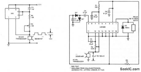
This ultrasonic transmit/receive circuit operates at 40 kHz. Control resistor R5 adjusts the frequency for best performance with the transducers used. (View)
View full Circuit Diagram | Comments | Reading(1618)
ULTRASONIC_TRANSCEIVER
Published:2009/7/9 0:35:00 Author:May
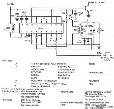
The LM1812 is a complete ultrasonic transceiver on a chip designed for use in a variety of pulseecho ranging applications. The chip operates by transmitting a burst of oscillations with a transducer, then using the same transducer to listen for a return echo. If an echo of sufficient amplitude is received, the LM1812 detector puts out a pulse of approximately the same width as the original burst. The closer the reflecting object, the earlier the return echo. Echos could be received immediately after the initial burst was trans-mitted, except for the fact that the transducer rings.
When transmitting, the transducer is excited with several hundred volts peak to peak, and it operates in a loudspeaker mode. Then, when the LM1812 stops transmitting and begins to receive, the transducer continues to vibrate or ring, even though excitation has stopped. The transducer acts as a microphone and produces an ac signal initially the same amplitude as the transmit pulse. This signal dies away as is gov-erned by the transducer's damping factor, but as long as detectable ringing remains, the LM1812's detector will be held on, masking any return echos. (View)
View full Circuit Diagram | Comments | Reading(2216)
SONIC_DEFENDER
Published:2009/7/8 23:49:00 Author:May
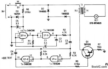


This oscillator-driver produces a deafening sound of about 3 kHz, modulated with a 10-Hz arble.BZ1 is a Matsushita EFB-RP34BZ. U1A and B generate the 10-Hz waveform that modulates the 3-kHz tone that is generated by U1C and D.Q1 drives the transducer through a 8-Ω:1-KΩ transformer. R4 might require slight changes ( ±1 kΩ) to optimize sound intensity.Warning: Could cause hearing loss if improperly used. (View)
View full Circuit Diagram | Comments | Reading(3806)
ULTRASONIC_RECEIVER
Published:2009/7/8 23:23:00 Author:May
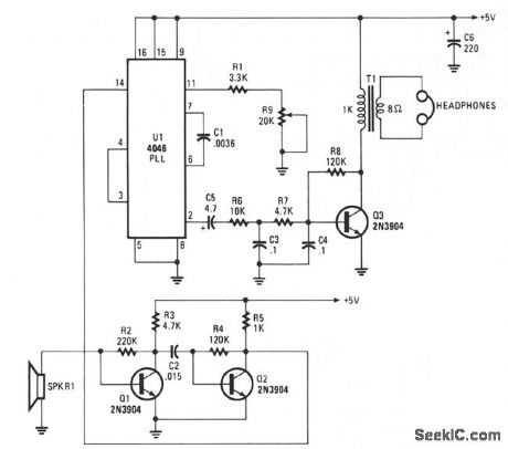
The 4046 PPL is used as the heart of a tunable ultrasonic receiver that can be used to locate unheard ultrasonic sounds. The receiver might also be used, along with a simple ultrasonic generator, to send and receive Morse code. The incoming ultrasonic signal is picked up by piezo speaker SPKRl, and amplified by transistors Q1 and Q2. The output is fed to the phase comparator input of U1 at pin 14. The chip's interval VCO is tuned by turning potentiometer R9.If a 20-kHz signal is picked up by SPKR1 and the VCO is tuned to produce a 19-kHz signal the difference output at pin 2 will be 1 kHz. That 1-kHz signal is amplified by Q3 and coupled through T1 to a pair of headphones. If the received frequency increases to 22 kHz, a 3-kHz tone is heard in the headphones. With the values given in the parts list for C1, R1, and R9, the VCO can be tuned from 12 to well over 42 kHz, which should cover just about anything the piezo sensor can respond to. (View)
View full Circuit Diagram | Comments | Reading(0)
4_to_20_ma_current_transmitter
Published:2009/7/21 2:50:00 Author:Jessie
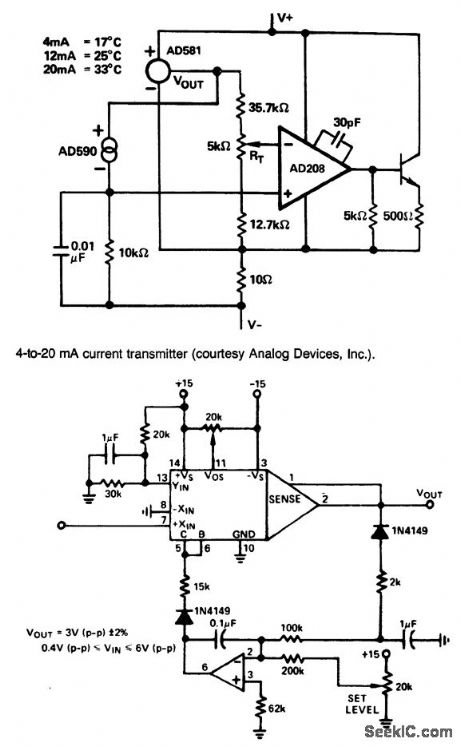
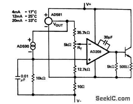
4-to-20 ma current transmitter (courtesy Analog Devices, Inc). (View)
View full Circuit Diagram | Comments | Reading(963)
| Pages:14/32 1234567891011121314151617181920Under 20 |
Circuit Categories
power supply circuit
Amplifier Circuit
Basic Circuit
LED and Light Circuit
Sensor Circuit
Signal Processing
Electrical Equipment Circuit
Control Circuit
Remote Control Circuit
A/D-D/A Converter Circuit
Audio Circuit
Measuring and Test Circuit
Communication Circuit
Computer-Related Circuit
555 Circuit
Automotive Circuit
Repairing Circuit