
Communication Circuit
Index 11
175_MHz_80_W_MOBILE_FM
Published:2009/7/14 1:38:00 Author:May
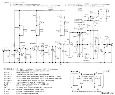
Uses Motorola of transistors optimized for 12.5-V FM operation. All stages are class C. Signal-splitting techniques in input and output matching networks of power output stage minimize problems of unequal load sharing and of matching to extremely low impedance levels. Overall gain is 26 dB, and efficiency is 49.5%.-J. Hatchett, Design Techniques for an 80 Watt, 175 MHz Transmitter for 12.5 Volt Operation, Motorola, Phoenix, AZ, 1972, AN-577, p 2. (View)
View full Circuit Diagram | Comments | Reading(1856)
TRANSISTORIZED_THYRATRON_RING_COUNTER
Published:2009/7/14 1:37:00 Author:May
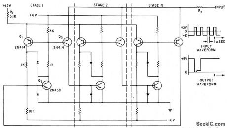
Each bistable circuit has two opposite-symmetry germanium transistors, two diodes, and four resistors. Additional transistor Q transfers conducting stage to next position when actuated by transfer pulse. Absence of capacitors gives high-speed operation. No bias current is required from ON stage to keep other stages cut off.-J. A. Pecar, Ring Counter Uses Transistors, Electronics, 34:4, p 49-51. (View)
View full Circuit Diagram | Comments | Reading(1388)
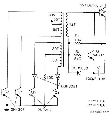
CAPACITOR_COUPLED_DRIVE_FOR_SWITCHING_TRANSISTOR
Published:2009/7/14 1:02:00 Author:May
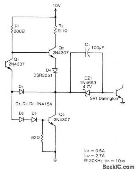
TRW SVT6062 power Darling-ton switching transistor is used in grounded-emitter connection in which negative bias required for turnoff is created by charging C1 during ON interval. Zener limits charge on C1 and provides path for base drive current to Darlington. Diodes give faster response to input signal by preventing Q3 from saturating. Grounding base of Q1 makes Darlington con duct, whereas high input level to Q1 initiates turnoff. Circuit will operate at pulse widths down to 5μs.-D. Roark, Base Drive Considerations in High Power Switching Transistors, TRW Power Semiconductors, Lawndale, CA, 1975, Application Note No. 120, p 7. (View)
View full Circuit Diagram | Comments | Reading(1123)
FOUR_CHANNEL_COMMUTATOR
Published:2009/7/14 0:48:00 Author:May
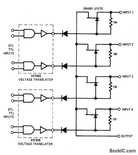
2N401 JFETs give ON resistance of less than 30 ohms for each channel along with low OFF current leakage, DS7800 voltage translators provide gate drives of 10 V to -20 V for JFETs while giving DTL/TTL compatibility, - FET Databook, National Semiconductor, Santa Clara, CA, 1977, p 6-26-6-36. (View)
View full Circuit Diagram | Comments | Reading(1038)
TRANSFORMER_DRIVE_FOR_SWITCHING_TRAN_SISTOR
Published:2009/7/14 0:44:00 Author:May
Transformer provides isolated base drive for high-speed high-power TRW SVT6062 power Darlington Q2. When 12-V secondary switches positive, C1 charges rapidly, after which base drive current is maintained at level determined by base-emitter voltage of Q2 and value of R1. During turnoff, transformer secondary goes to zero due to shorting of transformer primary by O3 and Q4. Base of Q1 is then forward-biased by capacitor and turned on, discharging C1 through base-emitter path of Q2-D. Roark, Base Drive Considerations in High Power Switching Transistors, TRW Power Semiconductors, Lawndale, CA, 1975, Application Note No. 120, p 6. (View)
View full Circuit Diagram | Comments | Reading(1010)
7625_AND_816_MHz
Published:2009/7/13 23:33:00 Author:May
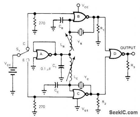
MCl0102 ECL quad NOR gate provides convenient switching between two crystal oscillators, as required for change from receive to transmit in transceiver. Output level of about 0.8 V P-P can easily drive 50-ohm load and is fully buffered from oscillator sections. Gate A provides bias for oscillator gates B and C. Use 270 ohms for R1-R3, Crystals are fifth overtone; YB is 81.6 MHz with 97 nH for LB and 39 pF for CB, and YC is 76.25 MHz with 104 nH for LC and 39 pF for CC.-G. Griesmyer, Clocked CMOS One-Shot Has No RC Time Constant, EDN Magazine, May 20, 1978, p 164 and 172.
(View)
View full Circuit Diagram | Comments | Reading(1100)
BINARY_WITH_STEERING_CIRCUIT_TRANSISTOR
Published:2009/7/13 22:12:00 Author:May
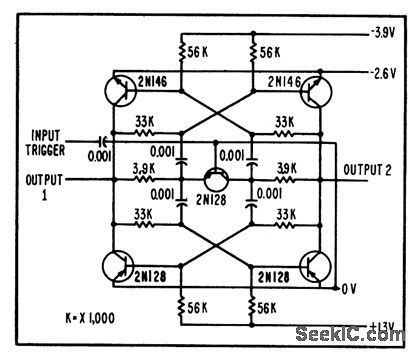
Input goes to steering transistor that replaces two back-to-back diodes normally used to drive bases of binary transistors through capacitive coupling. For-transistor binary flip-flop reduces total quiescent drain on batteries.-R.W. Rochelle. Cyclops Cores Simplify Earth-Satellite Circuits. Electronics.31:9,p56-63. (View)
View full Circuit Diagram | Comments | Reading(1589)
5_MHz_±_500_kHz
Published:2009/7/13 21:49:00 Author:May
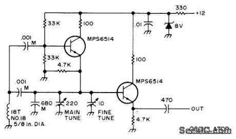
Developed for use as separate VFO control for transmitting and receiving frequencies in amateur transceiver. Capacitors marked M should be mica. Fine-tuning control covers ±20 kHz range. Will operate almost anywhere in HF range with appropriate change in coil. Output is 4 V P-P.-An Accessory VFO-the Easy Way, 73 Magazine, Aug. 1975, p 103 and 106-108. (View)
View full Circuit Diagram | Comments | Reading(1429)
4_CHANNELVHF_FM_SCANNER
Published:2009/7/13 21:40:00 Author:May
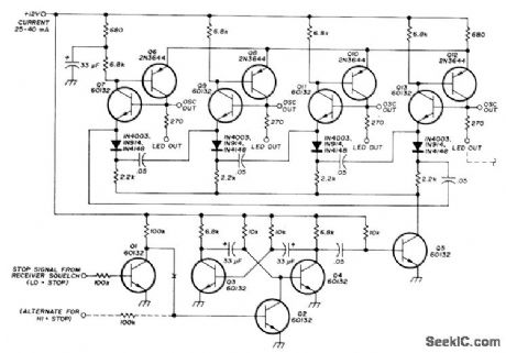
Discrete components permit simpler readout, with any number of channels and any desired scan rate. Operates directly from 10-15 V power supply without regulation, and has low current drain. Can be used with either positive or negative logic from squelch circuit, so scanning can be stopped with either positive or ground signal. Any voltage from a few volts up will stop scanning. Q3 and Q4 form astable MVBR operating at about 10 pulses per second. Q2 turns on to stop MVBR when base of Q2 is high. Inverter Q1 provides proper polarity of signal to operate Q2. Q6-Q13 form 4-stage ring counter. Pulsing by Q5 serves to pass high output from stage to stage in endless ring pattern. When squelch stops pulsing action, counter stops stepping and output of one counter stage stays high, providing 5-V output for enabling corresponding oscillator and driving LED for that channel, Article gives connections to oscillator for almost any FM transceiver or receiver, along with modifications for changing scan speed and number of channels.-J. Vogt, Improved Channel Scanner for VHF FMJ Ham Radio, Nov, 1974,p26-31. (View)
View full Circuit Diagram | Comments | Reading(1896)
AUTO_GUARDIAN_TRANSMITTER
Published:2009/7/13 21:17:00 Author:May
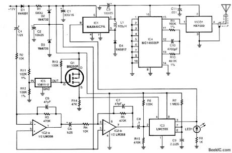
The circuit is powered by the vehicle's 12-V battery. A pair of zener diodes, D2 and D3, create two regulated voltage sources of 10.9 and 6.2 V. Integrated circuit IC2 contains a pair of identical op amps, which are cascaded. The negative input of IC2-a is ac-coupled to the 12-V bus so that it can detect a sudden sag in voltage caused by the current draw of the vehicle's dome lampswhen a door is opened. A change in battery voltage of 3 mV will cause a -6-V swing at the output of IC2-b, which is great enough to trigger IC3, a CMOS 555 timer chip. That IC is wired to operate as a one-shot pulse generator. An output pulse about 2[fr1/2] s long appears on pin 3 of IC3 when triggered by IC2-b. The output of IC3 is connected to the enable input of IC1, a switching-type voltage regulator. When IC1 is enabled, it outputs a regulated 3.3-Vdc power source for the transmitter portion of the circuit, encoder IC4 and transmitter module MOD1, When power is applied to the encoder, a series of pulse trains is generated that contain the address of the encoder. Those pulse trains are applied to pin 1 of the hybrid module to produce an RF signal with an on-off pulse modulation, sometimes called corn,plitude-shift keying. When the 2 1/2-s pulse time of IC3 is completed, the transmitter shuts down, returning to its dormant state.In order to prevent RE transmission while the vehicle is running, voltage detector IC5 uses R11 and R12 as a voltage divider to sense when the supply voltage rises above 12 V as a result of an alternator charging when the engine is running. Under that condition, the output of IC5 is open, turning off Q1. That holds the reset input of IC3 low, preventing the timer chip from responding to any trigger pulses from the amplifier. As a result, no transmission takes place. The HX1000 hybrid-transmitter module, MOD1, is a four-terminal device that contains a surface -acoustic -wave -stabilize d UHF oscillator. The oscillation frequency, 433.92 MHz, is stabilized and controlled by the resonant frequency of the internal surface-acoustic-wave filters, which also filter undesirable harmonics. The hybrid module is capable of delivering about I mW of power (0 dBm) into a 50-Ω load. It is connected to the trans-mitting antenna through a 50-Ω coaxial cable. (View)
View full Circuit Diagram | Comments | Reading(1659)
35_W_TRANSMITTER
Published:2009/7/13 5:17:00 Author:May
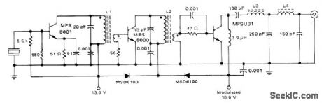
Class D circuit using economical plastic transistors operates from 12-V auto battery. 100% amplitude modulation requires about 2.5-W audio input. Modulator uses MSD6100 dual diode in modulated power supply system, with one diode in series with modulated supply voltage to MPS8000 driver to prevent driver from being down-modulated. Other diode maintains drive to final while final is being down-modulated, to make100% modulation easy to obtain. All coils are wound on 1/4-inch coil forms with No. 22 wire, with Carbonyl J 1/4× 3/8 inch cores in each. 2-turn secondaries are wound over bottom of primaries. L1 is 12 turns, L2 is 18, L3 is 7, and L4 is 5.-G. Young, A Class D Citizen's Band Transmitter Using Low-Cost Plastic Transistors, Motorola, Phoenix, AZ, 1975, AN-596. (View)
View full Circuit Diagram | Comments | Reading(1918)
TOROIDAL_TRANSFORMER
Published:2009/7/13 3:56:00 Author:May
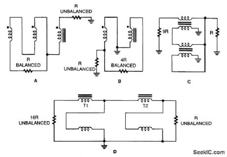
The several types of impedance matching transformers are∶1:1 baiun (A).4:1balun (B).9:1 unun (C).and 16:1 un-un (D) (View)
View full Circuit Diagram | Comments | Reading(2313)
THREE_COIL_CRYSTAL_RECEIVER
Published:2009/7/12 23:44:00 Author:May
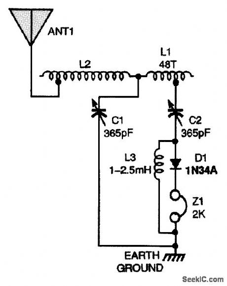
This circuit uses three inductors to increase the receiver's selectivity and sensitivity. Components L2 and C1 are used in an antenna impedance-matching circuit, while L1 and C2 operate in a series-tuned low-output impedance circuit that matches the impedance of the diode detector. A 1-to 2-mH inductor (L3), as in the previous circuit, offers dc continuity to the detector circuit. (View)
View full Circuit Diagram | Comments | Reading(1496)
13_GHz_ATV_TRANSMITTER
Published:2009/7/12 23:25:00 Author:May

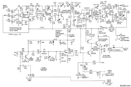
This TV transmitter operates from a +12-Vdc source and produces about 1 W peak power on sync tips. Output frequency is 1240 to 1300 MHz, but operation is possible to 1325 MHz (for U.K.band). Video interface is 1 V p-p/75 Ω negative sync; audio is 5 mV to 1 V @ 255 kΩ. For PAL operation, reduce the number of turns on L16 to 11 for 5.5-MHz sound.A kit of parts for this transmitter is available from North Country Radio, P.O. Box 53, Wykagyl Station, New Rochelle, NY 10804-0053A. (View)
View full Circuit Diagram | Comments | Reading(2946)
FOUR_MODE_FREQUENCY_COUNTER
Published:2009/7/12 23:01:00 Author:May
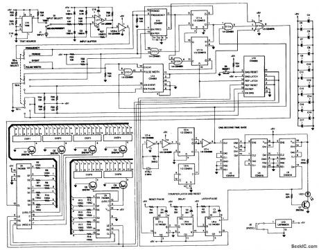
This counter can measure frequencies from 2 Hz to 1 MHz, time interval, and period, and count random events. A 74C926 and 74C925 are used as the counter, and these will drive a multiplexed LED display. A 2-MHz time base is used, and a divider chain is used to derive a 1-s gate. An LM339 op amp serves as the input buffer, and CD4000 series logic is used for gating and switching functions. (View)
View full Circuit Diagram | Comments | Reading(3385)
10_W_CW_TRANSCEIVER
Published:2009/7/12 22:59:00 Author:May
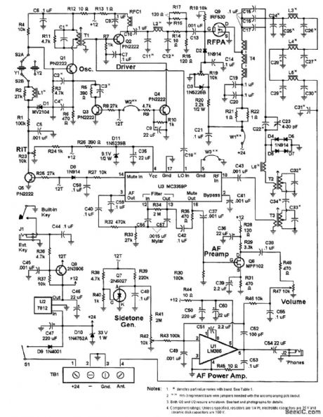
This transceiver can ioe operated on the 80-. 40-. or 30-m CW ham bands. A crystal oscillator drives a driver and RE PA delivering about 10 W output. The receiver uses an MC3359 IC and is fed LO from the crystal oscillator used for transmitting, and a varactor diode is used for incremental tuning (RIT) of the receiver. The unit also has a CW sidetone generator for ease of monitoring the transmitted CW signal. The power supply is 18 to 28 Vdc at 1 A. (View)
View full Circuit Diagram | Comments | Reading(3129)
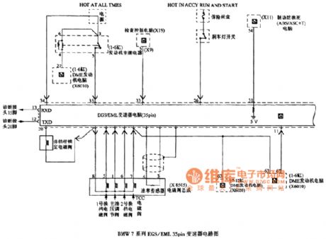
BMW7 Series EGS / EML 35pin Transmission Circuit (the 1st)
Published:2011/7/17 21:53:00 Author:Felicity | Keyword: BMW7 Series, EGS / EML 35pin, Transmission Circuit, (the 1st)
View full Circuit Diagram | Comments | Reading(1074)
FLASH_EEPROM_COMMUNICATOR
Published:2009/7/12 21:49:00 Author:May
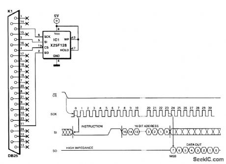
Modern equipment frequently uses serial EEPROMS to store data that must not be lost. With the circuit shown, it is possible to program or read such an IC via the Centronics port of a computer. Because the serial interface of a flash EEPROM is identical to that of an EEPROM, the two devices can communicate with each other. This means that the present circuit can be used for either device. The IC is enabled via CS (Chip Select). The command read followed by the address that needs to be read is set on to the high level is a little low, some 4.7 kΩ pull-up resistors can be added between the Centronics outputs and the positive supply line (not the SO line). (View)
View full Circuit Diagram | Comments | Reading(1350)
SERIAL_TRANSMITTER_CIRCUIT
Published:2009/7/12 21:48:00 Author:May
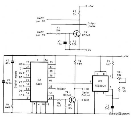
This circuit provides basic parallel-to-serial conversion, with the control inputs connected to provide a word format of 1 start bit, 8 data bits, 1 stop bit, and no parity. VR1 should provide operation at 1200 baud. Adjusting VR1 is just a matter of using trial and error to locate a setting that enables the computer to reliably decode the serial data. If a frequency meter is available, adjust VR1 for an output frequency of 19.2 kHz at pin 3 of IC2. (View)
View full Circuit Diagram | Comments | Reading(2661)
INFRARED_CODE_PRACTICE_TRANSMITTER
Published:2009/7/12 20:46:00 Author:May
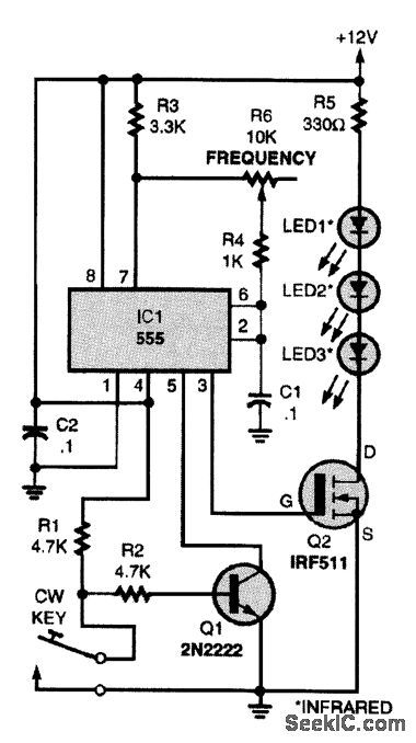
A 555 timer, IC1, is connected in an audio-oscillator circuit with its frequency set by potentiometer R6. Transistor Q1, with the CW key up, is biased on, thereby holding pin 5 of IC1 low and keeping it turned off. The 555 timer's output, at pin 3, ties to the gate of a power hexFET, Q2, which drives the three IR emitters, LED1 to LED3. Placing the CW key in the down position turns the 555 oscillator on. That sends out the audio tone signal via IR. (View)
View full Circuit Diagram | Comments | Reading(1451)
| Pages:11/32 1234567891011121314151617181920Under 20 |
Circuit Categories
power supply circuit
Amplifier Circuit
Basic Circuit
LED and Light Circuit
Sensor Circuit
Signal Processing
Electrical Equipment Circuit
Control Circuit
Remote Control Circuit
A/D-D/A Converter Circuit
Audio Circuit
Measuring and Test Circuit
Communication Circuit
Computer-Related Circuit
555 Circuit
Automotive Circuit
Repairing Circuit