
Communication Circuit
Index 9
AFSK_TONES
Published:2009/7/15 2:11:00 Author:Jessie
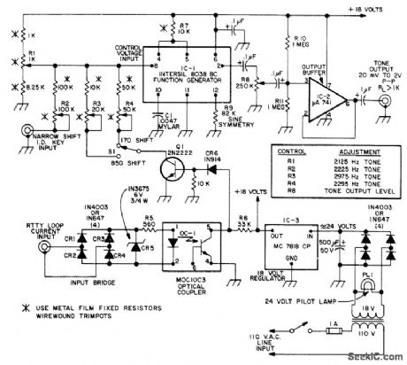
Generates tones needed for either 170- or 850-Hz frequency shift in automatic frequency-shift keying of B'FEY equipment. Independent adjustments are provided for each tone, Sine-wave output has constant amplitude, with excellent tone frequency stability. Circuit permits plug-in operation in any RTTY loop, independent of loop polarity or grounding. Article covers construction and adjustment.-J. C. Roos, Universal AFSK Generator, 73 Magazine, July 1974, p 37-40, 42, and 44-46.
(View)
View full Circuit Diagram | Comments | Reading(2129)
TELEPHONE_QUALITY_CODER_DECODER
Published:2009/7/14 4:54:00 Author:May
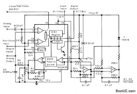
Uses Motorola MC3418 continuously variable slope delta modulator-demodulator IC to give over 50 dB of dynamic range for 1-kHz test at 37.7K bit rate. At this rate, 40 voice channels can be multiplexed on standard 1.544-megabit telephone carrier facility. IC includes active companding control and double integration for improved performance in encoding and decoding digital speech. Opamp types are not critical.- Continuously Variable Slope Delta Modulator/ Demodulator, Motorola, Phoenix, AZ, 1978, DS 9488. (View)
View full Circuit Diagram | Comments | Reading(1431)
FSK_DEMODULATOR_WITH_CARRIER_DETECT
Published:2009/7/14 5:00:00 Author:May
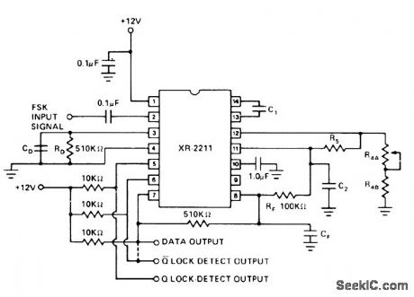


Exar XR-2211 FSK demodulator operating with PLL provides choice of outputs when carder is present; pin 5 goes low and pin 6 goes high when carrier is detected. With pins 6 and 7 connected, output from these pins provides data when FSK is applied but is low when no carrier is present. Circuit performance is independent of input signal strength over range of 2 mV to 3 VRMS. Center frequency is 1/C1R4 Hz, with values in farads and ohms. Choose frequency to fall midway between mark and space frequencies. Used in transmitting digital data over telecommunication I inks.- Phase-Locked Loop Data Book, Exar Integrated Systems, Sunnyvale, CA, 1978, p 57-61. (View)
View full Circuit Diagram | Comments | Reading(6779)
BALANCED_LIN_E_TRANSMISSION
Published:2009/7/14 4:38:00 Author:May
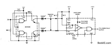
Transmits data at rates up to 0.5 MHz over twisted pair to Texas Instruments SN75152 dual-line receiver. Other section of receiver is identical and can handle additional twisted-pair input. Diodes in lines are required only for negative common-mode protection at driver outputs. System has high common-mode voltage capability. SN75450 is dual peripheral driver for high-current switching at high speeds.- The Linear and Interface Circuits Data Book for Design Engineers, Texas Instruments, Dallas, TX, 1973, p8-78. (View)
View full Circuit Diagram | Comments | Reading(1215)
CHROMA_PROCESSOR
Published:2009/7/15 3:04:00 Author:Jessie
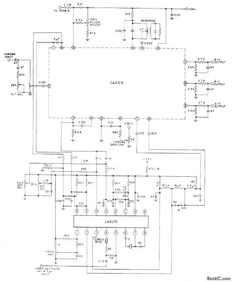
Combination of RCA CA3121E chroma amplifier/demodulator and CA3070 chroma signal processor provides automatic chroma control and color killer sensing along with other functions required for high-level B - Y, R - Y, and G - Y color difference signals having low impedances for driving highlevel R, G, and B output amplifiers.- Linear Integrated Circuits and MOS/FET's, RCA Solid State Division, Somerville, NJ, 1977, p 359-360. (View)
View full Circuit Diagram | Comments | Reading(1035)
LOW_NOISE_UHF_PREAMP
Published:2009/7/15 2:59:00 Author:Jessie

Special push-pull input stage using low-noise UHF transistors gives average preamp noise figure as low as 2.2 dB. Can be used with 300-ohm line of broad-band UHF antenna without usual balun trans-former or differential input stage. Balun is used after amplifier to transform push-pull output to input of single-ended second stage without de-grading noise figure. Developed for use with new deep-fringe-area UHF TV antenna having three flat in-line director elements, for over-the-air reception of UHF TV programs in areas previously having no watch able pictures.-J. E. Kluge, Advanced Antenna Design and an Ultra-low-Noise Preamplifier Extend UHF Viewing Area, IEEE Transactions on Broadcasting, March 1977, p 17-22.
(View)
View full Circuit Diagram | Comments | Reading(2485)
25_MHz_VIDEO_PREAMP
Published:2009/7/15 2:56:00 Author:Jessie
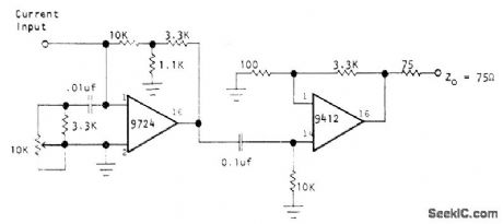
Uses Optical Electronics 9724 opamp for input stage and 9412 opamp for output stage. Current input can be from vidicon or image orthicon camera tube. Input compensation can be adjusted to provide aperture correction. Feedback network for input opamp minimizes effects of stray capacitance Values shown give 1-V output for 1-μA input.-“A 25 MHz Video Preamplifier-Line Drivel,” Optical Electronics, Tucson, AZ, Application Tip 10195. (View)
View full Circuit Diagram | Comments | Reading(1059)
OPTICALLY_COUPLED_DATA_LINK
Published:2009/7/14 4:28:00 Author:May
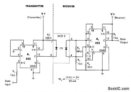
322 comparator at transmitter end of link drives LED of MCD 2 optoisolator which accepts TTL input. Receiver is similar comparator having additional biasing to match photodiode output of Output optoisolator. Complete system is noninverting,with delay of about 2 μs. Receiver can have any supply within 4.5-40 V range of 322. Transmitter should be matched to its supply voltage by selecting R2 according to equation shown.-W. G. Jung, IC Timer Cookbook, Howard VV. Sams, Indianapolis, IN, 1977, p 156-15.
(View)
View full Circuit Diagram | Comments | Reading(1160)
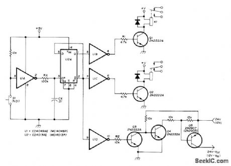
NIXIE_TUBE_RING_COUNTER
Published:2009/7/14 4:18:00 Author:May
Uses silicon controlled switches.- Transistor Manual, General Electric Co. 1964, p430. (View)
View full Circuit Diagram | Comments | Reading(996)
LOW_LEVEL_5_MC_TUNNEL_DIODE
Published:2009/7/14 4:17:00 Author:May
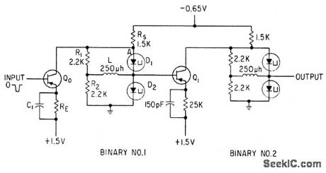
With 1N2933 germanium tunnel diode, power consumption is only 525 microwatts per transistor and binary stage. Circuit voltage and resistances are such that only one tunnel diode is in high-voltage state at a time. Silicon transistors, for coupling, can be pnp or npn.-E. Gottlieb and J. Giorgis, Tunnel-Diode Switching Circuits, Electronics, 36:27, p26-31. (View)
View full Circuit Diagram | Comments | Reading(1170)
TRANSFORMING__12_V_TO__15_V
Published:2009/7/14 4:16:00 Author:May
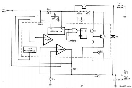
External PNP transistor Q3 and catch diode Q2 (types not critical) are used with Fairchild μA78S40 switching regulator so no pin of IC substrate has voltage more negative than substrate, which is grounded. Efficiency is 84% with 200-mA load. Output voltage ripple is 50 mV but can be reduced by increasing value of C0.-B. J. Apfel and D. B. Jones, Universal Switching Regulator Diversifies Power Subsystem Applications, Computer Design, March 1978, p 103-112. (View)
View full Circuit Diagram | Comments | Reading(961)
IMPROVING_TV_SOUND
Published:2009/7/15 4:57:00 Author:Jessie

AF signal from volume control of TV receiver is converted to FM signal by using BC107 transistor to frequency-modulate tunnel-diode oscillator operating within FM broadcast band. Oscillator output is fed through air-core transformer and coaxial line to FM receiver of high-fidelity sound system. Arrangement eliminates most of distortion introduced in power amplifier and loud-speaker of average TV set. Use shielding to keep unwanted FM radiation at minimum.-A. J. Smith, Improving Television Sound, Wireless World, Aug, 1973, p 373. (View)
View full Circuit Diagram | Comments | Reading(2479)
SYNC_SEPARATOR
Published:2009/7/15 4:55:00 Author:Jessie
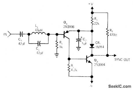
Input video having negative synchronizing pulses is applied to Q1 through 3.58-MHz notch filter Lt-Ct to remove color subcarrier components. Circuit is set up to conduct only on negative peaks, when Q1 Q2, and CR1 are all on, so feedback is 100% at this time. Negative peaks of output then follow input exactly. C2 acts as memory for negative peaks, storing their level between sync pulses.-W. Jung, An Operational Approach to Sync Separation, EDN/EEE Magazine, July 15, 1971, p 48-49. (View)
View full Circuit Diagram | Comments | Reading(0)
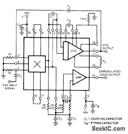
ANALOG_PLL_IN_FSK_DEMODULATOR
Published:2009/7/15 4:39:00 Author:Jessie
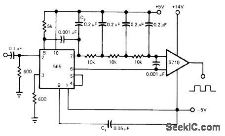
Developed for frequency-shift keying used in data transmission over wires, in which inputs vary carrier between two preset frequencies corresponding to low and high states of binary input signal. Circuit uses elaborate filter to separate modulated signal from carrier signal passed by PLL. 565 PLL provides reference for S710 comparator. Article gives design equations. -E. Murthi, Monolithic Phase-Locked Loops-Ana-logs Do All the Work of Digitals, and Much More, EDN Magazine, Sept. 5, 1977, p 59-64. (View)
View full Circuit Diagram | Comments | Reading(4120)
SINGLE_SUPPLY_HIGH_PRECISION_PLL
Published:2009/7/15 4:34:00 Author:Jessie
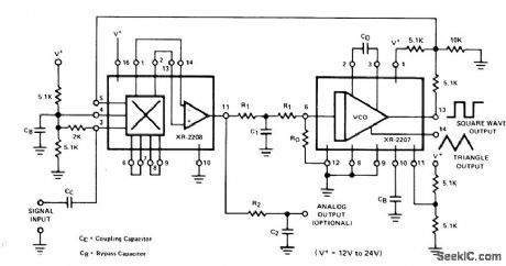
Combination of Exar XR-2207 VCO and XR-2208 operational multiplier is connected for operation from single 12-24 V supply for data communication and signal conditioning applications. Operating frequency range is 0.01 Hz to 100 kHz. Timing resistor R0 should be in range of 5K to 100K, and R1 should be greater than R0 For 10-kHz center frequency, C0 can be 0.01 μF and R0 can be 10K. R1 and C1 which determine tracking range and low-pass filter characteristics, are 45κ and 0.032 μF.- Phase-Locked Loop Data Book, Exar Integrated Systems, sunnyvale, CA, 1978, p62-64 (View)
View full Circuit Diagram | Comments | Reading(1361)
SOUND_SUBSYSTEM
Published:2009/7/15 4:32:00 Author:Jessie
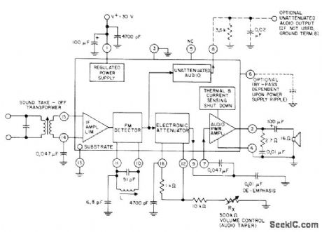
RCA CA3134 combines sound IF and audio output stages in single IC for use in TV receivers. Input is taken from sound IF output of receiver. Provides electronic volume control with improved taper. Alternate circuit shown provides unattenuated audio output.- Linear Integrated Circuits and MOS/ FETTs, RCA Solid State Division, Somenrville, NJ, 1977, p 368. (View)
View full Circuit Diagram | Comments | Reading(1185)
FSK_DETECTOR
Published:2009/7/15 4:04:00 Author:Jessie
Exar XR-5200 PLL IC is connected as modem suitable for Bell 103 or 202 data sets operating at data transmission rates up to 1800 bauds. Input frequency shift corresponding to data bit reverses polarity of DC out-put voltage of multiplier. DC level is changed to binary output pulse by gain block connected as voltage comparator. - Phase-Locked Loop Data Book, Exar Integrated Systems, Sunny-vale, CA, 1978, p 9-16. (View)
View full Circuit Diagram | Comments | Reading(1347)
VHF_VARACTOR_TUNER
Published:2009/7/15 3:55:00 Author:Jessie

DC bias voltages are used in place of mechanical switches for channel selection. Values for tuned circuit's depend on varactor diode used, With high-capacitance varactor diode, tuning voltage ranges from 4.3 V for channel 2 to 23 V for channel 13. Corresponding voltages for low-capacitance varactor are 2.2 V and 20.4 V. Tuner noise figure is in range of 4-5 dB.-J. Hopkins, Printed Circuit VHF TV Tuners Using Tuning Diodes, Motorola, Phoenix, AZ, 1972, AN-544A. p 4. (View)
View full Circuit Diagram | Comments | Reading(3370)
VIDEO_MODULATOR
Published:2009/7/15 3:52:00 Author:Jessie
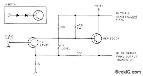
Developed for use between solid-state TV camera and VHF Engineering TX-432B crystal-controlled solid-state exciter to give simple amateur TV transmitter, For tube-type cameras, add 1N914 or other small-signal silicon diodes in series with input until modulator provides proper video swing Article gives construction details,-R E Taggart, Interested in Television, 73 Magazine,Oct 1977,p 164-174. (View)
View full Circuit Diagram | Comments | Reading(0)
TRANSISTORS_FOR_MIXER_AND_VR_TUBES
Published:2009/7/14 3:31:00 Author:May
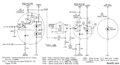
Premixer V6 in Drake T-4XB transmitter is replaced by dual-cascode MOSFETs, with CR4 protecting MOSFET from keyed-ground circuit. High-level mixer V7 operates over large dynamic range of signals coming from IF stage Output of mixer is low level, about 4 VRMS maximum. Decoupling capacitor C9 and choke High-level mixer V7 operates over large dynamic range of signals coming from IF stage Output of mixer is low level, about 4 VRMS L1 isolate JFET from high-voltage tube circuit.-H. J. Sartori, Solid-Tubes-a New Life for 0ld Designs, OST, April 1977, p 45-50. (View)
View full Circuit Diagram | Comments | Reading(1575)
| Pages:9/32 1234567891011121314151617181920Under 20 |
Circuit Categories
power supply circuit
Amplifier Circuit
Basic Circuit
LED and Light Circuit
Sensor Circuit
Signal Processing
Electrical Equipment Circuit
Control Circuit
Remote Control Circuit
A/D-D/A Converter Circuit
Audio Circuit
Measuring and Test Circuit
Communication Circuit
Computer-Related Circuit
555 Circuit
Automotive Circuit
Repairing Circuit