
Control Circuit
Index 122
OPAMP_DRIVES_POWER_DARLINGTONS
Published:2009/7/21 1:26:00 Author:Jessie
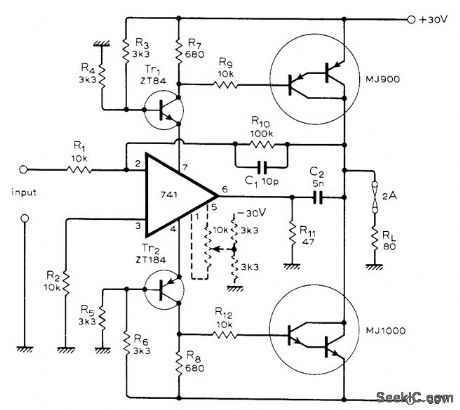
Differential outputs for Darlingtons are obtained by using power supply pins of 741 opamp. Tr1 and Tr2 can be any general-purpose transistors, and individual transistors can replace Darling-ton pairs. If circuit is used in servo system, add components shown in broken lines for zeroing of output offset. With values shown, 30 W can be delivered into 8 ohms from DC to 100 kHz at gain of 10 with less than 0.2% distortion.-K. Griffiths, Novel Power Amplifier, Wireless World, Dec. 1974, p 504. (View)
View full Circuit Diagram | Comments | Reading(2613)
44_VAC_DRIVE
Published:2009/7/21 1:27:00 Author:Jessie
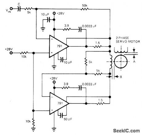
Uses two 791 power opamps, each rated for 10-W continuous dissipation, in AC bridge. Upper 791 has inverting gain of 10.Lower 791 inverts its output so 44 V P-P signal is applied across two-phase AC servomotor.-R. J. Apfel, Power Op Amps-Their Innovative Circuits and Packaging Provide Designers with More Options, EDN Magazine, Sept. 5, 1977, p 141-144. (View)
View full Circuit Diagram | Comments | Reading(709)
REMOTE_CONTROL_FOR_SERVO_POSITION
Published:2009/7/21 1:29:00 Author:Jessie
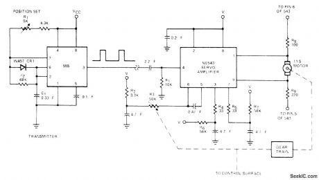
Setting of pot R, in circuit of remotely located 555 timer determines position of 11.5-ohm servomotor by feeding appropriate square-wave pulses over wire line to servoamplifier. - Signetics Analog Data Manual, Signetics, Sunnyvale, CA, 1977, p 727-728. (View)
View full Circuit Diagram | Comments | Reading(1654)
SCR_phase_control_circuit_with_a_PUT
Published:2009/7/21 2:04:00 Author:Jessie

SCR phase control circuit with a PUT. Relaxation oscillator Q2 provides conduction control of Q1 from 1 ms to 7.8 ms (courtesy Motorola Semiconductor Products Inc). (View)
View full Circuit Diagram | Comments | Reading(1120)
AC_RELAY
Published:2009/7/8 22:54:00 Author:May
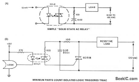
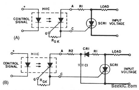
When zero voltage switching is not required, methods of providing this function are illustrated. The lowest parts count version of a solid-state relay is an optoisolator, the triac driver H11J. Unfortunately, the ability of the H11J to drive a load on a 60-Hz line is severely limited by its power dissipation and the dynamic characteristics of the detector. These factors limit applications to 30 - 50 mA resistive loads on 120 Vac, and slightly higher values at lower voltages. These values are compatible with neon lamp drive, pilot, and indicator incandescent bulbs; low voltage control circuits, such as furnace and bell circuits, if dV/dt are sufficient; but less than benign loads require a discrete triac.
The H11J1 triac trigger optocoupler potentially allows a simple power switching circuit utilizing only the triac, a resistor, and the optocoupler. This configuration will be sensitive to high values of dV/dt and noise on normal power-line voltages, leading to the need for the configuration shown in Fig. 67-14B, where the triac snubber acts as a filter for line voltage to the optocoupler.
Since the snubber is not usually used for resistive loads, the cost effectiveness of the circuit is compromised somewhat. Even with this disadvantage, the labor, board space, and inventory of parts savings of this circuit prove it cost-optimized for isolated logic control of power-line switching. In applications where transient voltages on the power line are prevalent, provisions should be made to protect the H11J1 from breakover triggering. (View)
View full Circuit Diagram | Comments | Reading(1377)
DC_LATCHING_RELAY
Published:2009/7/8 22:53:00 Author:May
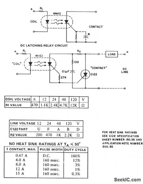

The H11C supplies the dc latching relay function and reverse polarity blocking, for currents up to 300 mA, depending on ambient temperature. For dc use, the gate cathode resistor can be supplemented by a capacitor to minimize transient and dV/dt sensitivity. For pulsating dc operation, the capacitor value must be designated to either retrigger the SCR at the application of the next pulse or prevent retriggering at the next power pulse. If not, random or undesired operation might occur. For higher current contacts, the H11C can be used to trigger an SCR capable of handling the current, as illustrated.
(View)
View full Circuit Diagram | Comments | Reading(1222)
ZERO_VOLTAGE_SWITCHING,SOLID_STATE_RELAY_WITH_ANTIPARALLEL_SCR_OUTPUT
Published:2009/7/8 22:51:00 Author:May
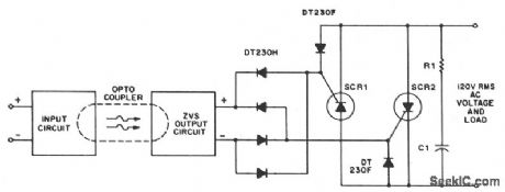
A higher line voltage can be used if the diode, varistor, ZVS, and power thyristor settings are at compatible levels. For applications beyond triac current ratings, antiparallel SCRs might be triggered by the ZVS network. (View)
View full Circuit Diagram | Comments | Reading(3413)
HT-7706 (Lighting) light control circuit
Published:2011/7/27 21:32:00 Author:TaoXi | Keyword: Lighting, light control
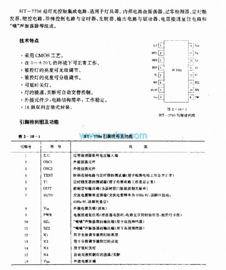
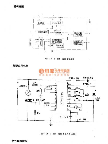
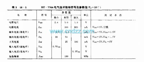
The HT-7706 is designed as the light control circuit that can be used in the lighting application. The internal circuit is composed of the oscillator, the zero crossing detector, the timing trigger, the button control circuit, the stage control circuit, the timer, the comparator, the output circuit, the driver, the power connection reset circuit and the di sound oscillator.
Features
The CMOS technology.It can operate normally in the environment of 0 to +70℃.The brightness of the controlled light is stepless adjusting mode.The brightness of the controlled light has two stages.The delay turn-off function.The automatic alternate turn-on and turn-off.
(View)
View full Circuit Diagram | Comments | Reading(682)
NORMALLY_OPEN_AND_NORMALLY_CLOSED_DC_SOLID_STATE_RELAYS
Published:2009/7/8 22:42:00 Author:May
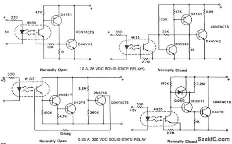
The phototransistor and photodarlington couplers act as dc relays in saturated switching at currents up to 5 mA and 50 mA, respectively. When higher currents or higher voltage capabilities are required, additional devices are required to buffer or amplify the photocoupler output. The addition of hysteresis to provide fast switching and stable pick-up and drop-out points can be easily implemented simultaneously.These circuits provide several approaches to implement the dc relay function and serve as practical, costeffective examples. (View)
View full Circuit Diagram | Comments | Reading(1757)
A Circuit of High-performance Infrared Remote Switch
Published:2011/8/1 3:22:00 Author:Zoey | Keyword: High-performance, Infrared, Remote Switch
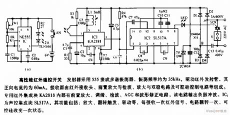
This transmitter uses a connected 555 multi-vibrator to drive the infrared infrared lauch tube, the vibrator's oscillation frequency is about 36kHz and its positive current is about 60mA. The receiver is composed of a infrared receiver head, a pre-amplification and detection circuit, an amplification and bistable circuit and a SCR control circuit. The specilized infrared integrated block KA2818 consists of a pre-amplification, tuning, detection, AGC waveform correction circuit, which inputs negative pulse wave. IC2 is a voice control integrated block SL517A, it has such functions as amplification, trigger flipand drive, etc. Everytime it receives infrared signal, the circuir will filp one time, and the SCR will change its state one time. (View)
View full Circuit Diagram | Comments | Reading(791)
SOLID_STATE_ZERO_VOLTAGE_SWITCHING_ZVS_CIRCUITS
Published:2009/7/8 22:26:00 Author:May
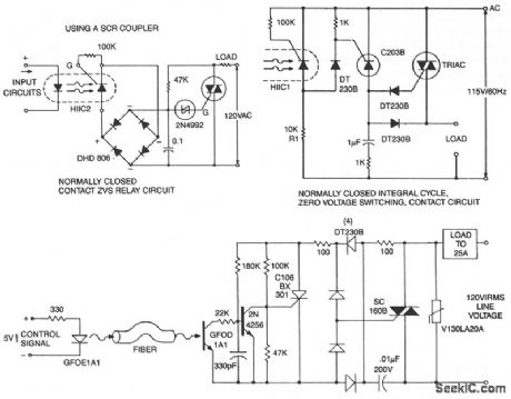
This circuit is effective for lamp and heater loads. Some circuits driving reactive loads require integral cycling and zero-voltage switching-when an identical number of positive and negative half cycles of voltage are applied to the load during a power period. The circuit, although not strictly a relay because of the three-terminal power connection, performs the integral cycle ZVS function when interfaced with the previous coil circuits.
Fiber optics offers advantages in power control systems. Electrical signals do not flow along the non-conducting fiber, minimizing shock hazard to both operator and equipment. EMI/RFI pick up on the fiber is nonexistent-although high gain receiver circuits might require shielding, eliminating noise pick-up errors caused by sources along the cable route. Both ac and dc power systems can be controlled by fiber optics using techniques similar to the optoisolator solid-state relay. Triac triggering is accomplished through the C106BX301, a low gate trigger current SCR, switching line voltage derived current to the triac gate via the full-wave rectifter bridge. The primary difference between ftber optics solid-state relay circuits and optoisolator circuits is the gain; photo currents are much smaller.
(View)
View full Circuit Diagram | Comments | Reading(1293)
KEYLESS_LOCK
Published:2009/7/8 22:26:00 Author:May
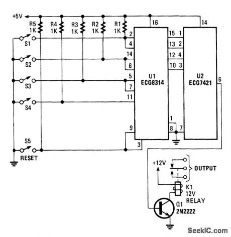
The circuit uses a four-bit latch(U1).What makes the circuit sequential is that the set input of the firstbit latch is tied to the reset of the second bit latch,and so forth.That ensures that any bit latched will be reset by the prevtous bit latch.The ECG8314 also has a master reset (pin 9)that is tiedto the first bit latch reset (pin 3),which provides an added measure of security for the lock.
The outputs of U1 are fed to a four-input AND gate(U2),then to Q1(used as switching transistor),which is used to drive relay K1. The EGC8314 has an enable low (pin) that can be used as a timing circuit,If that is desired. (View)
View full Circuit Diagram | Comments | Reading(1069)
Difference_of_squares_circuit_using_an_AD534_multiplier_divider_chip
Published:2009/7/21 4:39:00 Author:Jessie
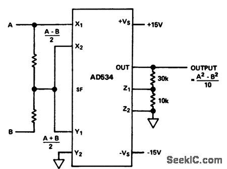
Difference of squares circuit using an AD534 multiplier/divider chip (courtesy Analog Devices, Inc.). (View)
View full Circuit Diagram | Comments | Reading(588)
HIGH_VOLTAGE_AC_SWITCHER
Published:2009/7/8 22:19:00 Author:May
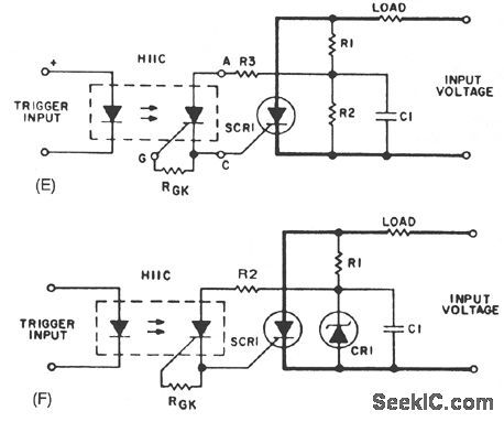
A guide for selecting the component values would consist of the following steps:
· Choose C1 in a range of 0.05 to 1 μR The maximum value might be limited by the recharging time constant (RL + R1) C1 while the minimum value will be set by the minimum pulse width required to ensure SCR latching.· R2 is determined from peak gate current limits, if applicable, and minimum pulse width requirements.· Select a zener diode. A 25-V zener is a practical value, since this will meet the usual gate requirement of 20 V and 20 Ω. This diode will also eliminate spurious triggering because of voltage transients.· Photon coupler triggering is ideal for the SCR's driving inductive loads. By ensuring that the LASCR latches on, it can supply gate current to SCR1 until it stays on.· Component values for dc voltage are easily computed from the following formulae: EIN-VZR1 = — IG where: V =zener voltage P(R1) =IG·(EIN-VZ) P(ZENER) =IG·VZ (View)
View full Circuit Diagram | Comments | Reading(0)
_HIGH_VOLTAGE_AC_SWITCHER
Published:2009/7/8 22:16:00 Author:May
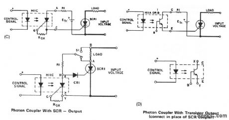
In Fig. 67-1C, R1 can be connected to Point A, which will remove the voltage from the coupler after SCR1 is triggered, or to Point B so that the coupler output will always be biased by input voltage. The former is preferred since it decreases the power dissipation in R1. A more practical form of SCR triggering is shown in Fig. 67-1F. Trigger energy is obtained from the anode supply and stored in C1. Coupler voltage is limited by the zener voltage. This approach permits switching of higher voltages than the blocking voltage capability of the output device of the photon coupler. To reduce the power losses in R1 and to obtain shorter time constants for charging C1, the zener diode is used instead of a resistor. (View)
View full Circuit Diagram | Comments | Reading(742)
HIGH_VOLTAGE_AC_SWITCHER
Published:2009/7/8 22:13:00 Author:May
A basic circuit to trigger an SCR is shown in Fig. 67-1A. This circuit has the disadvantage that the blocking voltage of the photoncoupler output device determines the circuit-blocking voltage, irrespective of higher main SCR capability.
Adding capacitor C1 to the circuit, as shown in Fig. 67-1B, will reduce the dV/dt seen by the photon-coupler output device. The energy stored in C1, when discharged into the gate of SCR1, will improve the di/dt capability of the main SCR.
Using a separate power supply for the coupler adds flexibility to the trigger circuit; it removes the limitation of the blocking voltage capability of the photon-coupler output device. The flexibility adds cost and more than one power supply nftght be necessary for multiple SCRs if no common reference points are available. (View)
View full Circuit Diagram | Comments | Reading(968)
Triac_control_circuit_using_an_ECG776_zero_voltage_switch_IC
Published:2009/7/21 4:48:00 Author:Jessie
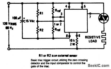
Triac control circuit using an ECG776 zero voltage switch IC. Resistor R2 must be the external sensor for the internal short and open protection to be operative. Select the triac from the ECG5600 series for the particular application (courtesy GTE Sylvania Incorporated). (View)
View full Circuit Diagram | Comments | Reading(2329)
TOY_TRAIN_CONTROL
Published:2009/7/23 21:44:00 Author:Jessie
With L1-C1 tuned to one of five r-f channels (100, 140, 180, 220 and 255 kc), pair of scr's drives train either forward or in reverse, depending on polarity of r-f signal pulse applied to rails by control station. Five-channel transmitter permits simultaneous control of five different trains, each having receiver tuned to different frequencies. Scr characteristics eliminate jackrabbit starts.-S. B, Gray, Appliances and Housewares, Electronics, 36:20, p 46-49. (View)
View full Circuit Diagram | Comments | Reading(771)
LOW_NOISE_UHF_TV_TUNER
Published:2009/7/23 21:53:00 Author:Jessie
Input is tunable from 470 to 890 Mc, and output is 45 Mc.Gain is 3 to 9 db over uhf band, with typical noise figure of 7 to 9 db.-Texas Instruments Inc., Solid-State Communications, McGraw-Hill, N.Y., 1966, p 299. (View)
View full Circuit Diagram | Comments | Reading(891)
Fast_charge_controllers_for_NiCcld_NiMH
Published:2009/7/27 0:25:00 Author:Jessie
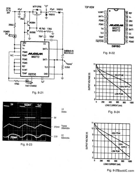
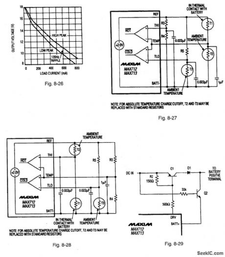
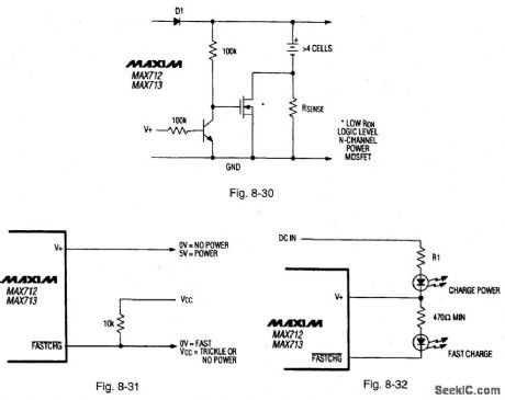
Figure 8-21 shows a MAX713 connected to provide a fast charge for two cells at 1 A. Higher charge currented and greater number of cells can be accommodated by changing RSENSE and the PGMO-PCM3 connections (as described in the date sheet).Figure 8-22 shows the pin connections and Fig. 8-23 shows the circuit waveforms. Notice that the circuit of Fig. 8-21 cannot service a loud while charging. The Fig. 8-21 circuit is usually used with an ac-to-dc wall cube (transformer,bridge rectifier, and capactior in a plug-in package).Figures 8-24.8-25,and 8-26 show the characteristics of three consumer-product wall cubes. when selecting a wall cube, be sure that the lowest dip in the wall-cube voltage. Figure 8-27 shows the connections for controlling charge cutoff with negative-temperature-coefficient (NTC) thermistors. Use the same model of thermistor for T1 and T2 so that both have the same nominal resistance. The voltage at TEMP is 1 V (referred to batt-) when the battery is at ambient temperature.some battery pavks might come with a temperature-detecting thermistor connected to the negative terminal of the battery pack. In this case, use the connections shown in Fig. 8-28. T2 and T3 can be replaced with standard resistors if absolute temperature cutoff is acceptable.The absolute maximum voltage rating for the BATT+ input voltage must be limited by external circuits when DC IN is not applied, as shown in Fig. 8:29. Rsense causes a small efficiency loss during battery use. The efficiency loss is significant only if Rsense is much greater than the internal resistance of the battery pack. The circuit of Fig. 8-30 can be used to shunt Rsense whenever power is removed from the charger. Figure 8-31 shows a circuit used to indicate charger status, with logic-level outputs. Figure 8-32 shows an LED drive circuit that indicates charger status. MAXIM NEW RELEASES DATA BOOK, 1994, P. 4-60, 4-61, 4-63, 4-64. (View)
View full Circuit Diagram | Comments | Reading(866)
| Pages:122/312 At 20121122123124125126127128129130131132133134135136137138139140Under 20 |
Circuit Categories
power supply circuit
Amplifier Circuit
Basic Circuit
LED and Light Circuit
Sensor Circuit
Signal Processing
Electrical Equipment Circuit
Control Circuit
Remote Control Circuit
A/D-D/A Converter Circuit
Audio Circuit
Measuring and Test Circuit
Communication Circuit
Computer-Related Circuit
555 Circuit
Automotive Circuit
Repairing Circuit