
Control Circuit
Index 167
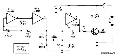
CAPACITANCE_OPERATED_ALARM_TO_FOIL_PURSE_SNATCHERS
Published:2009/6/24 23:01:00 Author:Jessie
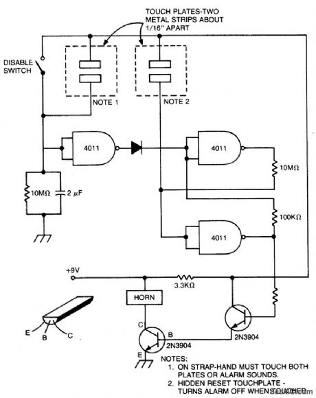
Aslong as touch plates (1) are touched together,the alarm is off. If not held for about 30 seconds,the alarm goes off. The circuit can be disabled with switch or by touching the plates (2),The alarm is battery operated by a bicycle horn. (View)
View full Circuit Diagram | Comments | Reading(1317)
ADJUSTABLE_LIGHT_DETECTION_SWITCH
Published:2009/6/24 22:45:00 Author:May


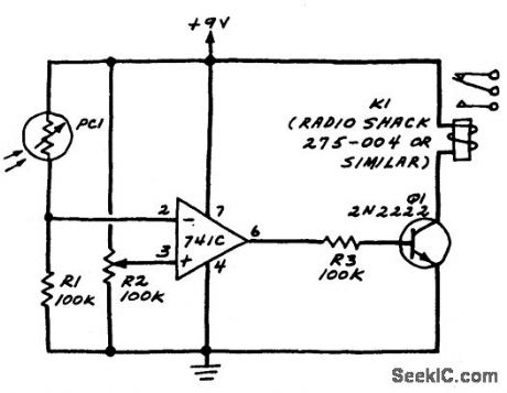
R2 sets the circuit's threshold. When the light intensity at PCI's surface is decreased, the resistance of PC1 a cadmium-sulfide photoresistor is increased. This decreases the voltage atthe inverting input of the 741. When the reference voltage atthe 741's noninverting input isproperly adjusted via R2, the comparator will switch from low to high when PC1 is darkened. This turns on Q1 which, in turn, pulls in relay K1. (View)
View full Circuit Diagram | Comments | Reading(1088)
NI_CAD_DISCHARGE_LIMITER
Published:2009/6/24 22:25:00 Author:May
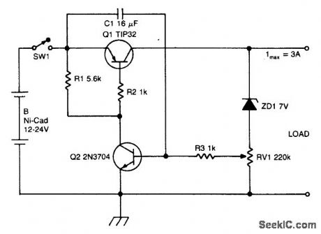
The circuit disconnects the battery from the load when output voltage falls below a pre-set level. C1 charges through R1 and turns on Q2. Collector current flows through R2 tuming Q1 on and battery is connected to the load. When the output voltage falls below a point set by RV1, Q2 turns off, Q1 tums off and further discharge of the battery is prevented. (View)
View full Circuit Diagram | Comments | Reading(740)
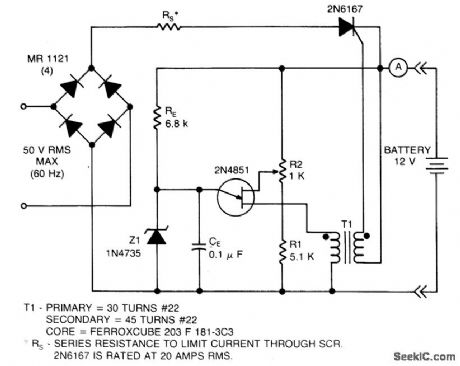
12_V_BATTERY_CHARGER_CONTROL_20_AMPS_RMS_MAX
Published:2009/6/24 22:01:00 Author:May
View full Circuit Diagram | Comments | Reading(1116)
WINDSHIELD_WIPER_HESITATION_CONTROL_UNIT
Published:2009/6/24 21:49:00 Author:May
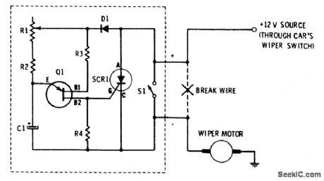

This circuit uses the 555 timer in the asta-ble or oscillatory mode. The length of time the timer is off is a function of the values of C1, R2, and R3. The potentiometer which controls the amount of hesitation . (Approximately 2 to 15 seconds.) R2 provides a minimum time delay when R3 is at its zero ohms position. (View)
View full Circuit Diagram | Comments | Reading(958)
VIDEO_SWITCH
Published:2009/6/24 21:48:00 Author:May
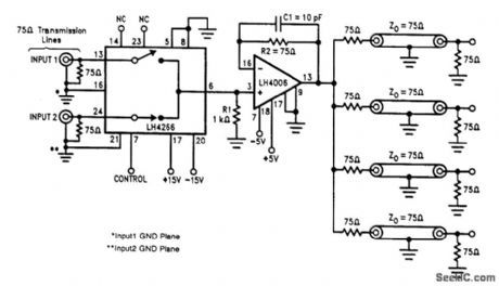
Using National Semiconductor LH4266 and LH4006, this circuit switches one of two inputs to four output (75Ω) lines. (View)
View full Circuit Diagram | Comments | Reading(1)
FREQUENCY_SWITCHER
Published:2009/6/24 21:32:00 Author:May
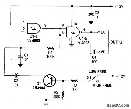
This transistor can achieve frequency switching in this CMOS astable oscillator. (View)
View full Circuit Diagram | Comments | Reading(0)
ADJUSTABLE_VFO_TEMPERATURE_COMPENSATOR
Published:2009/6/24 21:45:00 Author:Jessie
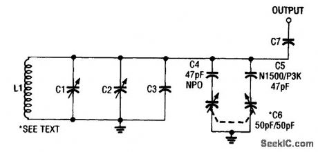
Use of a differential capacitor allows temperature compensation of LC circuit using an NPO and N1500 ceramic. C6 is a differential capacitor that has two stators and one common rotor. When one capacitance (stator) is maximum, the other is minimum. L1, C1, C2, and C3 are tuning, trimming, and fixed capacitors, respectively. (View)
View full Circuit Diagram | Comments | Reading(1354)
VARIABLE_DUTY_CYCLE_OSCILLATOR
Published:2009/6/24 21:42:00 Author:Jessie

Using a potentiometer and steering diodes, this 1.2-kHz oscillator will provide 1 to 99% duty cycle. Vary C1 to change frequency. (View)
View full Circuit Diagram | Comments | Reading(1397)
INDICATOR_AND_ALARM
Published:2009/6/24 21:24:00 Author:May
View full Circuit Diagram | Comments | Reading(985)
FREQUENCY_SWITCHER
Published:2009/6/24 21:32:00 Author:Jessie
This transistor can achieve frequency switching in this CMOS astable oscillator. (View)
View full Circuit Diagram | Comments | Reading(1605)
ULTRASONIC_MOTION_DETECTOR
Published:2009/6/24 21:32:00 Author:Jessie
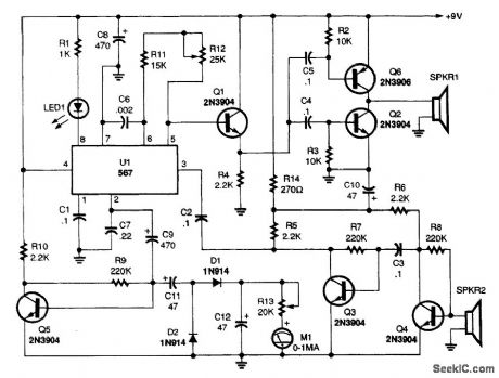
A 567 PLL IC operates in a dual-function mode as a signal generator and an FM receiver. The 567's square-wave output at pin 5 is coupled to the base of Q1, and from Q1's emitter to the input of the power amplifier (Q2 and Q6). The output drives the piezo speaker, SPKR1.
The receive portion of the circuit operates as follows: transistors Q3 and Q4 are connected in a two-stage, high-gain, audio-frequency amplifier circuit, with the input connected to a second piezo speaker (SPKR2) operating as a sensitive microphone. The amplifier's output is coupled to the 567's input at pin 3. When an in-band signal is received, the LED lights.
The 567's FM output is coupled from pin 2 to the input of a very-low-frequency single-transistor amplifier, Q5. The amplifier's output at Q5's collector drives a voltage-doubler circuit (C11, D1, D2, and C12). The dc output feeds a 0- to 1-mA analog meter.
By placing the two pigzo speakers one foot apart and aiming them in the same direction, toward a nonmoving solid object, the signal from the transmitter's speaker urill reflect back into the receiver's speaker, and the frequency at the 567's input will be the same as the one being transmitted.
The ac output at pin 2 is zero when the outgoing and incoming frequencies are the same. How-ever, when the signal is reflected from a moving object, the received frequency will be either lower or higher than the transmitted one. If the object is moving away from the speakers, the received fre-quency will be lower; if the object is moving toward the speakers, the frequency will be higher.
The pin-2 signal is fed through a 470-pF capacitor to the base of Q5, where the signal is ampli-fied and fed to a voltage doubler, and then on to a meter circuit.
If you wish, the voltage doubter and meter can be removed and replaced with headphones connected between the negative side of C11 and circuit ground. That will allow you to listen to the difference-frequency signal as objects move in front of the speakers. (View)
View full Circuit Diagram | Comments | Reading(4868)
CMOS_VFO
Published:2009/6/24 21:31:00 Author:Jessie
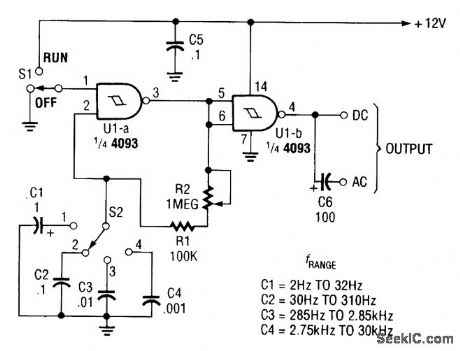
The circuit shown has a frequency range of 2 Hz to 30 kHz. R2 is a linear or log potentiometer. (View)
View full Circuit Diagram | Comments | Reading(1535)
CRYSTAL_OSCILLATOR
Published:2009/6/24 21:28:00 Author:Jessie
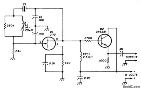
Circuit NotesStable VXO using 6-or 8-MHz crystals uses a capacitor and an inductor to achieve frequency pulling on either side of series resonance. (View)
View full Circuit Diagram | Comments | Reading(215)
PROXIMITY_ALARM
Published:2009/6/24 21:10:00 Author:May
View full Circuit Diagram | Comments | Reading(0)
TOUCH_SWITCH
Published:2009/6/24 21:10:00 Author:May
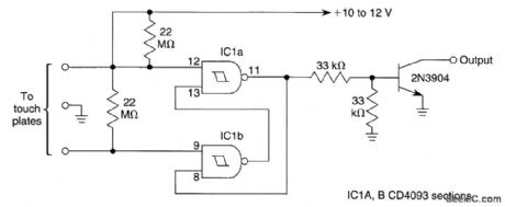
Two NAND Schmitt triggers are used as a flip-flop to produce a bridged touch switch. (View)
View full Circuit Diagram | Comments | Reading(0)
SIMPLE_TIMED_TOUCH_SWITCH
Published:2009/6/24 21:06:00 Author:May
This circuit produces an output for a time approximately equal to time constant R3/C1.
IC1,IC2 CD4011 quad NAND gateIC3 CD4066 quad bilateral switchC1 47-μF, 25-V electrolytic capacitorC2 100-μF, 25-V electrolytic capacitorC3 220-μF, 25-V electrolytic capacitorC4470-μF, 25-V electrolytic capacitorC5,C6,C7 0.1-μF capacitorRI,R3,R4,R6100-kΩ,1/4-W 5% resistorR7,R9,R10,R12 100-kΩ,1/4-W 5% resistorR2,R5,R8,R11 (View)
View full Circuit Diagram | Comments | Reading(0)
LOCAL_OSCILLATOR_FOR_DOUBLE_BALANCED_MIXERS
Published:2009/6/24 21:19:00 Author:Jessie
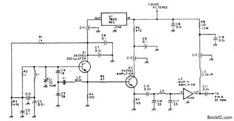
This circuit has an amplifier to supply +10 dBm to an SBL series (Mini-circuits) or similar type doubly-balanced mixer assembly. This circuit has values shown for =80- to 90-MHz crystals, although values of oscillator circuit constants can be scaled for higher or lower frequencies. (View)
View full Circuit Diagram | Comments | Reading(1545)
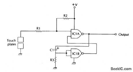
SIMPLE_TOUCH_SWITCH
Published:2009/6/24 21:05:00 Author:May
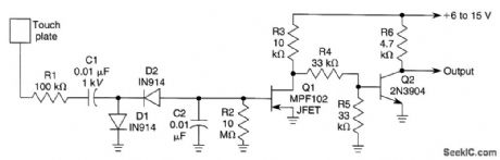
Q2 is held cut off since Q1 normally is conducting. When the touch plate is contacted by a large object (human body, etc.), stray 60-Hz pickup is rectified by D1 and D2, and produces a negative voltage across R2-C2 and the gate of Q1. Q1 cuts off, causes Q2 to conduct, and the output goes low. (View)
View full Circuit Diagram | Comments | Reading(0)
VARIABLE_WIEN_BRIDGE_OSCILLATOR
Published:2009/6/24 21:15:00 Author:Jessie
This circuit uses a single potentiometer to tune a 300- to 3000-Hz range. A FET op amp is used at A1 and A2. The upper frequency limit is determined by the gain-bandwidth product of the op amps. (View)
View full Circuit Diagram | Comments | Reading(1375)
| Pages:167/312 At 20161162163164165166167168169170171172173174175176177178179180Under 20 |
Circuit Categories
power supply circuit
Amplifier Circuit
Basic Circuit
LED and Light Circuit
Sensor Circuit
Signal Processing
Electrical Equipment Circuit
Control Circuit
Remote Control Circuit
A/D-D/A Converter Circuit
Audio Circuit
Measuring and Test Circuit
Communication Circuit
Computer-Related Circuit
555 Circuit
Automotive Circuit
Repairing Circuit