
Control Circuit
Index 181
WHISTLE_SWITCH
Published:2009/6/18 22:29:00 Author:May
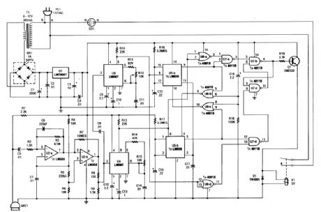
At the heart of the whistle switch are a pair of tone detectors, each of which is built around an LM567 tone decoder, which are supported by a ntinimum of additional components. This whistle switch is designed to respond to only two or more occur-rences of a specific tone, or sequence of tones, within a specified period to prevent false triggering. Depending on the relay used, various ac loads can be controlled. Microphone MIC1 picks up the sound and U2 amplifies the signal and feeds it to tone decoders U3 and U4. These devices trigger U5-a and U5-b and the logic circuits that drive relay K1. (View)
View full Circuit Diagram | Comments | Reading(2055)
SLEEP_MODE_CIRCUIT
Published:2009/6/18 22:08:00 Author:May
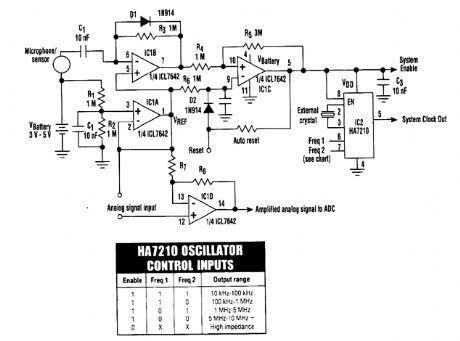
The HA7210 oscillator IC combines with an ICL7642 quad CMOS op amp to produce a sleep-mode control circuit. The circuit is put into the sleep mode with a logic high applied to the Reset input or with an RC timer for automatic reset. The system is awakened by a signal from the microphone/sensor. (View)
View full Circuit Diagram | Comments | Reading(1824)
SHUTDOWN_CIRCUIT
Published:2009/6/18 21:37:00 Author:May
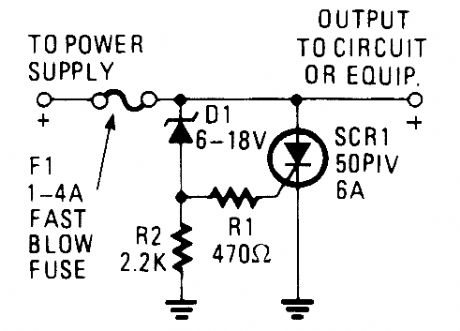
Many modern devices have shutdown circuits that are designed to remove power from the de-vice under power when the voltage rises above a predetermined threshold. This one blows a fuse to protect the device under power. (View)
View full Circuit Diagram | Comments | Reading(922)
RESETTABLE_SHUTDOWN_CIRCUITS
Published:2009/6/18 21:37:00 Author:May
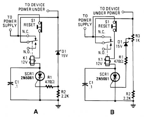
If your circuits experience frequency overvoltage conditions, continually replacing blown fuses can get pretty expensive. However, this shutdown circuit overcomes that deficiency by replacing the fuse with a relay and a low-current SCR. When the input voltage rises above the threshold set by the Zener diode (D1), a current of suf-ficient magnitude is applied to the gate of SCR1, which turns it on. That draws current through the relay coil and energizes it, which swings its commutator to its normally open contact, and disrupts power to the circuit under power. Switch S1, a normally closed pushbutton switch, is used to reset the circuit; it does so by interrupting power to the relay. When S1 is pressed, the relay's wiper arm returns to the normally closed position, restoring power to the connected circuit.If you deal with a number of circuits that have different burn-out levels, try the circuit in B. That circuit variation, a variable trip-point shutdown circuit, allows you to adjust the shutdown threshold to whatever level you desire. The circuit adjustment allows for the 30% variance in the trip point.The zener diode should be selected to have a voltage rating that is slightly lower than the minimum desired threshold voltage. (View)
View full Circuit Diagram | Comments | Reading(947)
LATCHING_TOUCH_SWITCH_USING_CD4066B
Published:2009/6/18 4:13:00 Author:May
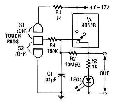
When touch switch S1 is activated, R4 is driven high, and the control voltage goes high, which latches the switch. When S2 is activated, R4 goes low and the control voltage goes low, which deactivates the switch. (View)
View full Circuit Diagram | Comments | Reading(934)
TOUCH_ON_ONLY_SWITCH
Published:2009/6/18 4:11:00 Author:May
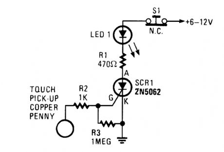
This touch on-only switch can be triggered into conduction by electrical means, and can only be reset by way of a mechanical switch. When the touch terminal is contacted by a finger, the SCR turns on and illuminates LED1. (View)
View full Circuit Diagram | Comments | Reading(862)
TOUCH_SWITCH_II
Published:2009/6/18 4:10:00 Author:May
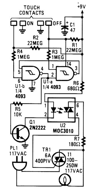


When the touch-on contacts are bridged, pin 6 of U1-b goes low, which forces its output (the set output) at pin 4 to go high. That high divides along two paths: in one path, the output is applied to pin 2 of UI-a, which causes its out-put at pin 3 to go low. That low is, in turn, ap-plied to pin 5 of UI-b, which latches the gate in a high output state. In the other path, the out-put of U1-b is used to drive Q1. When Q1 turns on, U2's internal LED lights, which turns on its internal, light-sensitive, triac-driver (diac) out-put element. The triac driver feeds gate current to TRI, causing it to turn on, and light the lamp (11).When the off contact is bridged, UI-a's out-put switches and latches high, causing UI-b's output to go low, turning off the lamp. (View)
View full Circuit Diagram | Comments | Reading(377)
TOUCH_SWITCH_I
Published:2009/6/18 4:04:00 Author:May
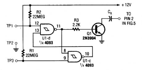
Two NAND Schmitt triggers are connected in a flip-flop configuration to produce a bridged touch-activated switch. (View)
View full Circuit Diagram | Comments | Reading(1128)
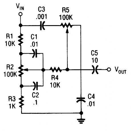
BASS_TONE_CONTROL
Published:2009/6/18 3:58:00 Author:May
The frequency dependence of the capacitor's impedance permits this circuit to boost the bass frequencies. (View)
View full Circuit Diagram | Comments | Reading(1336)
SWITCH_CLOSURE_CIRCUIT
Published:2009/6/18 3:58:00 Author:May
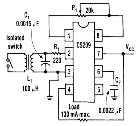
A standard proximity detector circuit for the Cherry Semiconductor CS209 IC can detect an iso-lated switch closure by adding a few tums of wire around the circuit's inductor (Radio Shack 273-102). Moreover, the technique doesn't require any isolated power (see the figure). With the switch open, the potentiometer P1 is adjusted until the output switches off. When the switch is closed, the Q of the circuit changes and the output turns on. Capacitor C1 should be silvered mica, and poten-tiometer P1 should be a multiturn type such as the Boums 3006P-1-203. A 9-V supply can be used for Vcc. (View)
View full Circuit Diagram | Comments | Reading(1137)
TREBLE_TONE_CONTROL
Published:2009/6/18 3:58:00 Author:May

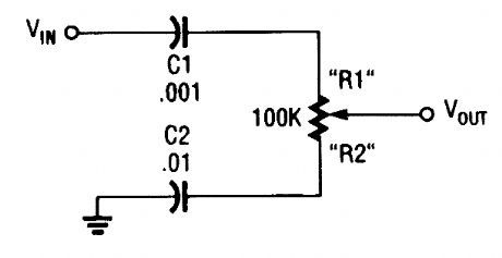
The treble control has capacitors placed in series with the potentiometer. (View)
View full Circuit Diagram | Comments | Reading(732)
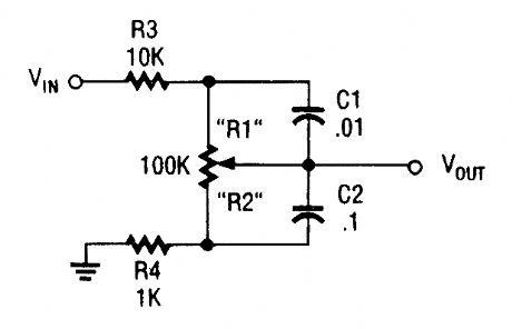
COMBINED_BASS_AND_TREBLE_CONTROLS
Published:2009/6/18 3:57:00 Author:May
Bass and treble circuits can be combined to form a two-control here. (View)
View full Circuit Diagram | Comments | Reading(887)
LONG_DELAY_PERIOD_TIMER
Published:2009/6/18 3:37:00 Author:May
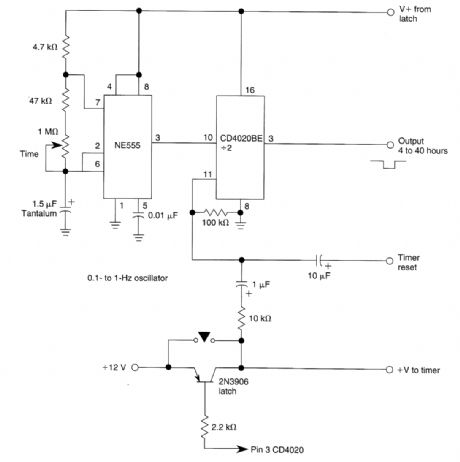
This method of obtaining a 4 to 40 hour timing period from a 555 IC can be further expanded to produce even longer delays with equal accuracy. (View)
View full Circuit Diagram | Comments | Reading(1284)
VCR_VIDEO_DETECTOR_CONTROLLER
Published:2009/6/18 3:36:00 Author:May
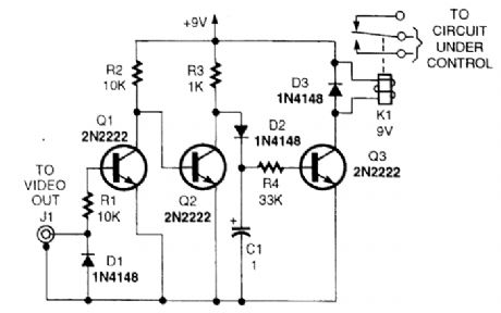
This circuit uses the video output from a VCR or camera to control a relay. Video turns on Q1, cutting off Q2, allowing Q3 to be forward biased, activating relay K1. You can use the timer in your VCR and this unit to generate long time delays as well. (View)
View full Circuit Diagram | Comments | Reading(1498)
TRANSMIT_KEYER_INTERFACE_CIRCUITS
Published:2009/6/18 3:31:00 Author:May

These circuits are for use with Morse kevers and identifiers They can be used to interface various devices with the identifier circuitry (View)
View full Circuit Diagram | Comments | Reading(735)
THREE_STAGE_SEQUENTIAL_TIMER_
Published:2009/6/18 3:14:00 Author:May
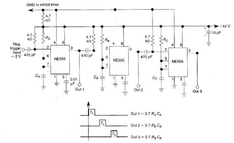
By using three 555 ICs, three sequential pulses can be generated. Output 3 can be connected back to trigger input to achieve astable operation. (View)
View full Circuit Diagram | Comments | Reading(1503)
TELE_TIMER
Published:2009/6/18 3:11:00 Author:May
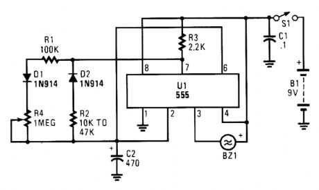
The circuit is built around a 555 oscillator/ timer. The circuit provides two time periods. The long-running time period is adjustable from about 1 to 10 minutes, and the short time period is pre-set to about three seconds.
Here's how the dual timer operates. When the power is switched on, C2 begins to charge through R3, R1, Dl, and R4 to start the long-term timer period. When the voltage across C2 reaches the 555's internal switching point, the long-term timer times out, discharging C2 throughR2, D2, and pin7 ofthe 555. Duringthat time, pin 3 of the 555 is pulled to ground, acti-vating the piezo sounder.To set the short time period to about four seconds, use a 10 k resistor for R2, and for about twenty seconds use a 47 k resistor. The timing capacitor, C2, should be a good-quality, low-leakage unit. (View)
View full Circuit Diagram | Comments | Reading(979)
BATTERY_PACK_AND_REVERSE_POLARITY_PROTECTION
Published:2009/6/18 3:03:00 Author:May
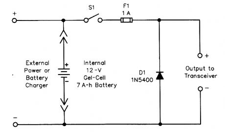
Schematic diagram and parts list for the reverse-polarity protection circuit D1 1N5400 silicon diodeF1 1-A fast-acting fuseS1 SPST rocker switch (View)
View full Circuit Diagram | Comments | Reading(2273)
SIMPLE_TIME_DELAY_CIRCUIT
Published:2009/6/18 3:02:00 Author:May
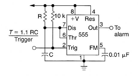
Rotating the potentiometer wiper will change the time delay from the 555 IC. (View)
View full Circuit Diagram | Comments | Reading(994)
ELECTRONICS_NOW
Published:2009/6/18 2:59:00 Author:May


This timer circuit uses a 555IC timer and three 74LS193 counters to drive an LED display. S1 is activated by one person, who tums on piezo buzzer BZ1 via Q1 and also starts the clock; S1 is acti-vated by the other person being timed. This shuts off the timer, and the number of LEDs lit indicate, in binary form, the elapsed time. (View)
View full Circuit Diagram | Comments | Reading(2439)
| Pages:181/312 At 20181182183184185186187188189190191192193194195196197198199200Under 20 |
Circuit Categories
power supply circuit
Amplifier Circuit
Basic Circuit
LED and Light Circuit
Sensor Circuit
Signal Processing
Electrical Equipment Circuit
Control Circuit
Remote Control Circuit
A/D-D/A Converter Circuit
Audio Circuit
Measuring and Test Circuit
Communication Circuit
Computer-Related Circuit
555 Circuit
Automotive Circuit
Repairing Circuit