
Control Circuit
Index 163
REMOTE_RING_EXTENDER_SWITCH
Published:2009/6/25 22:15:00 Author:May
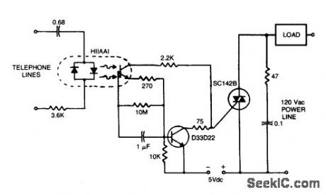


The circuit can operate lamps and buzzers from the 120V, 60 Hz power line while main-taining positive isolation between the tele-phone line and the power line. Use of the iso-lated tab triac simplifies heat sinking by removing the constraint of isolating the triac heat sink from the chassis. (View)
View full Circuit Diagram | Comments | Reading(788)
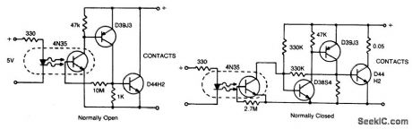
10_A_25_Vdc_SOLID_STATE_RELAYS
Published:2009/6/25 21:57:00 Author:May
View full Circuit Diagram | Comments | Reading(696)
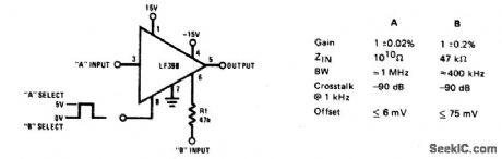
TWO_CHANNEL_SWITCH
Published:2009/6/25 21:56:00 Author:May
View full Circuit Diagram | Comments | Reading(717)
HIGH_FREQUENCY_SWITCH
Published:2009/6/25 21:53:00 Author:May

The 2N4391 provides a low ON resistance of 30 ohm and a high OFF impedance (<0.2 pF) when off. With proper layout and an ideal switch, the performance stated above can be readily achieved. (View)
View full Circuit Diagram | Comments | Reading(0)
DIFFERENTIAL_ANALOG_SWITCH
Published:2009/6/25 21:52:00 Author:May
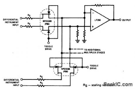
The NPD5566 monolithic dual is used in a differential multiplex application where Rd,coN) should be closely matched. Since Rd,coN) for the monolithic dual tracks at better than ±1% over wide temperature ranges (- 25℃ to +125℃), this makes it an unusual but ideal choice for an accurate multiplexer. This close tracking greatly reduces errors due to common-mode signals. (View)
View full Circuit Diagram | Comments | Reading(0)
TRIAC_ZERO_VOLTAGE_SWITCHING
Published:2009/6/25 21:55:00 Author:Jessie
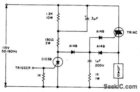
The triac will be gated on at the start of the positive half cycle by current flow through the 3 μF capacitor as long as the C103 SCR is off. The load voltage then charges up the 1 μF capacitor so that the triac will again be ener-gized during the subsequent negative half cycle of line voltage. A selected gate triac is required because of the triggering mode. (View)
View full Circuit Diagram | Comments | Reading(1724)
HIGH_FREQUENCY_SWITCH
Published:2009/6/25 21:53:00 Author:Jessie
The 2N4391 provides a low ON resistance of 30 ohm and a high OFF impedance (<0.2 pF) when off. With proper layout and an ideal switch, the performance stated above can be readily achieved. (View)
View full Circuit Diagram | Comments | Reading(1392)
DIFFERENTIAL_ANALOG_SWITCH
Published:2009/6/25 21:52:00 Author:Jessie
The NPD5566 monolithic dual is used in a differential multiplex application where Rd,coN) should be closely matched. Since Rd,coN) for the monolithic dual tracks at better than ±1% over wide temperature ranges (- 25℃ to +125℃), this makes it an unusual but ideal choice for an accurate multiplexer. This close tracking greatly reduces errors due to common-mode signals. (View)
View full Circuit Diagram | Comments | Reading(1817)
HIGH_TOGGLE_RATE_HIGH_FREQUENCY_ANALOG_SWITCH
Published:2009/6/25 21:49:00 Author:Jessie
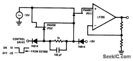
Commutator circuit provides low tmpedance gate drive to the PN4091 analog switch for both on and offdrive conditions.This circuit also approaches the ideal gate drive conditions for high frequency signal handling by providing a low ac impedance for off drive and high ac impedance for on drive to the PN4091 (View)
View full Circuit Diagram | Comments | Reading(1260)
DTL_TTL_CONTROLLED_BUFFERED_ANALOG_SWITCH
Published:2009/6/25 21:48:00 Author:Jessie
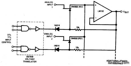
This analog switch uses the 2N4860 JFET for its 25 ohm ron and low leakage. The LM102 serves as a voltage buffer. This circuit can be adapted to a dual trace oscilloscope chopper. The DS7800 monolithic IC provides adequate switch drive controlled by DTL/TTL logic levels. (View)
View full Circuit Diagram | Comments | Reading(1276)
SQUAREWAVE_OSCILLATOR
Published:2009/6/25 21:43:00 Author:Jessie
View full Circuit Diagram | Comments | Reading(664)
SIMPLE_TRIANGLE_SQUARE_WAVE_OSCILLATOR
Published:2009/6/25 21:42:00 Author:Jessie
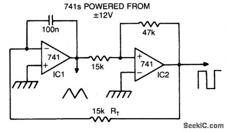
Circuit Notes By making Rr variable it IS possible to alter the operating frequency over a 100 to 1range,Versatile triangle/square wave oscillator has a possible frequency range of 0.1 Hz to 100 kHz. (View)
View full Circuit Diagram | Comments | Reading(6709)
SOUND_OPERATED_TWO_WAY_SWITCH
Published:2009/6/25 21:20:00 Author:May
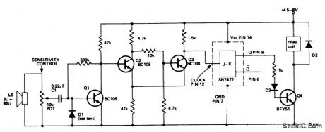
This circuit operates a relay each time a sound of sufficient intensity is made, thus one clap of the hands will switch it one way, a second clap will revert the circuit to the origi-nal condition. Q2 and Q3 form a Schmitt trigger. TheJK flip-flop is used as a bistable whose output changes state every time a pulse is applied to the clock input (pin 12). Q4 allows the output to drive a relay. (View)
View full Circuit Diagram | Comments | Reading(0)
SOUND_ACTIVATED_RELAY
Published:2009/6/25 21:19:00 Author:May
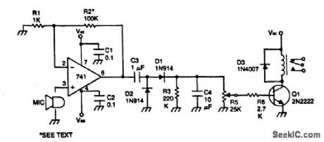
The device remains dormat (in an off con-dition) until some sound causes it to turn on. The input stage is a 741 operational amplifier connected as a noninverting follower audio amplifier. Gain is approximately 100. To increase gain raise the value of R2. The amplified signal is rectified and filtered to a dc level by R4. Then R5 is set to the audio level desired to activate the relay. (View)
View full Circuit Diagram | Comments | Reading(902)
PRECISION_RECTIFIERS
Published:2009/6/25 21:23:00 Author:Jessie
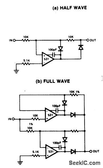
View full Circuit Diagram | Comments | Reading(552)
AUDIO_OPERATED_RELAY
Published:2009/6/25 21:15:00 Author:May
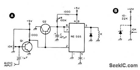
Q1 and Q2 are general purpose transis-tors. The 10 K input pot is adjusted to a point just short of where Q1 turns on as indicated by K pulling in. K is any 5 V reed relay. With the values shown for R (100 K) and C (47 μF), timing values from.05 to slightly over 5 sec-onds can be achieved. B shows the addition o f a 22 K series resistor to the 10 K input pot if a 12 V supply is used. A suitable 12 V reed relay must be used at K. (View)
View full Circuit Diagram | Comments | Reading(0)
ULTRA_PRECISE_LONG_TIME_DELAY_RELAY
Published:2009/6/25 21:12:00 Author:May

Circuit NotesPredictable time delays from as low as 0.3 milliseconds to over 3 minutes are obtainable without resorting to a large value electrolytic-type timing capacitor. Instead, a stable low leakage paper or mylar capacitor is used and the peak point urrent of the timing UJT (Q1) is effectively reduced, so that a large value emit-ter resistor (R1) may be substituted. (View)
View full Circuit Diagram | Comments | Reading(881)
SIMPLE_TIME_DELAY
Published:2009/6/25 21:15:00 Author:Jessie

View full Circuit Diagram | Comments | Reading(0)
AUDIO_OPERATED_RELAY
Published:2009/6/25 21:15:00 Author:Jessie
Q1 and Q2 are general purpose transis-tors. The 10 K input pot is adjusted to a point just short of where Q1 turns on as indicated by K pulling in. K is any 5 V reed relay. With the values shown for R (100 K) and C (47 μF), timing values from.05 to slightly over 5 sec-onds can be achieved. B shows the addition o f a 22 K series resistor to the 10 K input pot if a 12 V supply is used. A suitable 12 V reed relay must be used at K. (View)
View full Circuit Diagram | Comments | Reading(1928)
LONG_DURATION_TIME_DELAY
Published:2009/6/25 21:14:00 Author:Jessie
View full Circuit Diagram | Comments | Reading(1)
| Pages:163/312 At 20161162163164165166167168169170171172173174175176177178179180Under 20 |
Circuit Categories
power supply circuit
Amplifier Circuit
Basic Circuit
LED and Light Circuit
Sensor Circuit
Signal Processing
Electrical Equipment Circuit
Control Circuit
Remote Control Circuit
A/D-D/A Converter Circuit
Audio Circuit
Measuring and Test Circuit
Communication Circuit
Computer-Related Circuit
555 Circuit
Automotive Circuit
Repairing Circuit