
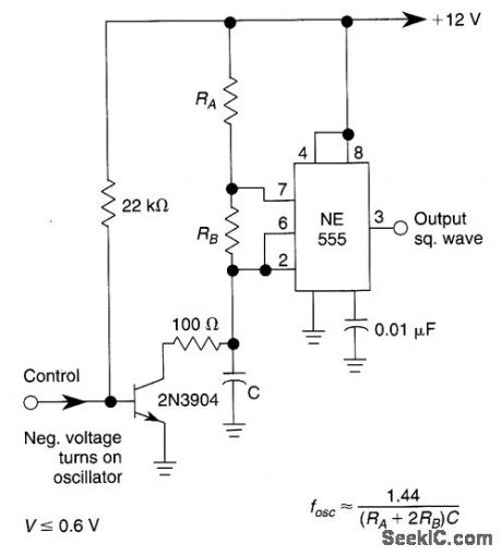
Control Circuit
Index 168
FAST_TURN_ON_DELAYED_OFF_RELAY_CIRCUIT
Published:2009/6/24 5:41:00 Author:Jessie
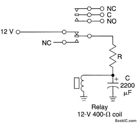
C is a large capacitor that has a charge time of RSUPPLY C, assuming RSUPPLY <Rcoil, The discharge time will be Rcoil C neglecting relay coil inductance. With C = 10,000 μF and Rcoil 500 Ω, a release time constant of 5 seconds might be obtained. Many relays will hold in until the coil current decays to 25% of the pull-in current so that the actual time constant depends on the relay holding current. (View)
View full Circuit Diagram | Comments | Reading(1365)
TRANSISTOR_RELAY_DRIVER
Published:2009/6/24 5:37:00 Author:Jessie
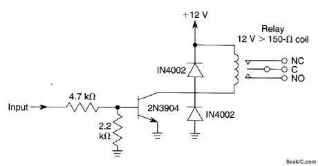
An input of 4 V or greater will drive this relay circuit. (View)
View full Circuit Diagram | Comments | Reading(1793)
LATCHING_RELAY_DRIVER
Published:2009/6/24 5:37:00 Author:Jessie
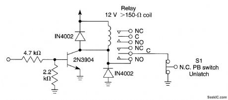
An input of 4 V or greater will drive this circuit. When the relay pulls in, one pair of contacts is used to latch the relay closed. It will remain closed until S1 is pressed. (View)
View full Circuit Diagram | Comments | Reading(1793)
HIGH_MPEDANCE_RELAY_DRIVER
Published:2009/6/24 5:35:00 Author:Jessie
A CMOS gate is used to drive a switching transistor and relay. (View)
View full Circuit Diagram | Comments | Reading(1260)
TRANSISTOR_RELAY_DRIVER
Published:2009/6/24 5:37:00 Author:May
An input of 4 V or greater will drive this relay circuit. (View)
View full Circuit Diagram | Comments | Reading(0)
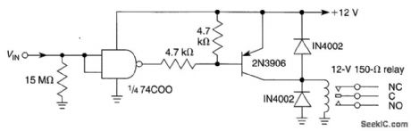
LATCHING_RELAY_DRIVER_FOR+12_V_LOADS
Published:2009/6/24 5:33:00 Author:Jessie
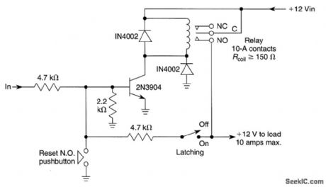
A 4-V signal will cause the relay to pull in when Q1 turns on. Latching is obtained by feedback through a 4.7-kΩ resistor. A switch is used to select latching or nonlatching operation. A NO pushbutton releases the circuit. (View)
View full Circuit Diagram | Comments | Reading(1633)
LATCHING_RELAY_DRIVER
Published:2009/6/24 5:37:00 Author:May
An input of 4 V or greater will drive this circuit. When the relay pulls in, one pair of contacts is used to latch the relay closed. It will remain closed until S1 is pressed. (View)
View full Circuit Diagram | Comments | Reading(0)
HIGH_MPEDANCE_RELAY_DRIVER
Published:2009/6/24 5:35:00 Author:May
A CMOS gate is used to drive a switching transistor and relay. (View)
View full Circuit Diagram | Comments | Reading(0)
LATCHING_RELAY_DRIVER_FOR+12_V_LOADS
Published:2009/6/24 5:33:00 Author:May
A 4-V signal will cause the relay to pull in when Q1 turns on. Latching is obtained by feedback through a 4.7-kΩ resistor. A switch is used to select latching or nonlatching operation. A NO pushbutton releases the circuit. (View)
View full Circuit Diagram | Comments | Reading(0)
BASIC_OSCILLATOR_CIRCUITS
Published:2009/6/24 21:12:00 Author:Jessie
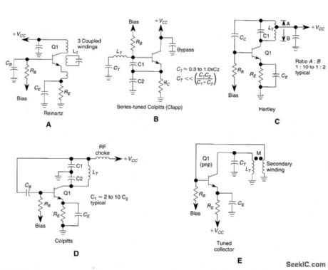
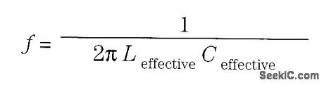
Five basic types of LC oscillators are shown. The frequency can be changed by using the formula:where Leffective =equivalent inductance Ceffective =equivalent capacitance (View)
View full Circuit Diagram | Comments | Reading(1455)
PROXIMITY_ALARM
Published:2009/6/24 21:10:00 Author:Jessie
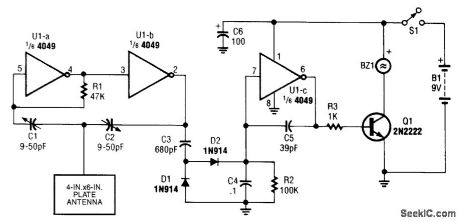
View full Circuit Diagram | Comments | Reading(1641)
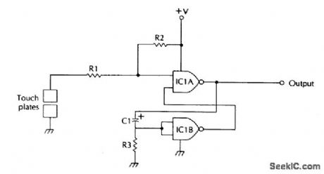
TOUCH_SWITCH
Published:2009/6/24 21:10:00 Author:Jessie
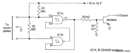
Two NAND Schmitt triggers are used as a flip-flop to produce a bridged touch switch. (View)
View full Circuit Diagram | Comments | Reading(2686)
CAPACITIVE_SENSOR_SYSTEM
Published:2009/6/24 21:08:00 Author:Jessie
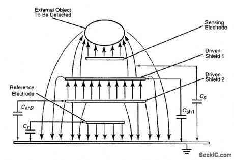
This figure illustrates the electric-field configuration of a capacitive proximity sensor of the ca-paciflector type. It includes a sensing electrode driven by an alternating voltage, which gives rise to an electric field in the vicinity of the electrode; an object that enters the electric field can be de-tected by its effect on the capacitance between the sensing electrode and electrical ground.Also, it includes a shielding electrode (in this case, driven shield 1), which is excited via a volt-age follower at the same voltage as that applied to the sensing electrode to concentrate more of the electric outward from the sensing electrode, increasing the sensitivity and range of the sensor. Be-cause the shielding electrode is driven via a voltage follower, it does not present a significant elec-trical load to the source of the alternating voltage.In this case, the layered electrode structure also includes a reference electrode adjacent to ground, plus a second shielding electrode (driven shield 2), which is excited via a voltage follower at the same voltage as that applied to the reference electrode. Driven shield 2 isolates the reference electrode from the electric field generated by driven shield 1 and the sensing electrode so that a nearby object exerts no ca[acitive effect on the reference electrode.The excitation is supplied by a crystal-controlled oscillator and applied to the sensing and ref-erence electrodes via a bridge circuit. Fixed capacitors C1 and C2 (or, alternatively, fixed resistors RI and R2) are chosen to balance the bridge; that is, to make the magnitude of the voltage at sens-ing-electrode node S equal the magnitude of the voltage at reference-electrode node R.The voltages at S and R are peak-detected and fed to a differential amplifier, which puts out volt-age 7, proportional to the difference between them. When no object intrudes into the electric field of the sensing electrode, the bridge remains in balance, and Vu - 0. When an object intrudes, it changes CS, unbalances the bridge, and causes Vu to differ from zero. The closer the object comes to the sensing electrode, the larger (Vu) becomes.An additional output voltage KVr is available, where K is the amplification and Vr is the voltage on the reference electrode. (View)
View full Circuit Diagram | Comments | Reading(3009)
PRECISION_LF_OSCILLATOR
Published:2009/6/24 21:07:00 Author:Jessie
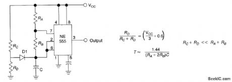
Using R1, R7, and D1 to preset C1 to one third of the supply voltage, this circuit avoids a longer first cycle period than subsequent cycles. (View)
View full Circuit Diagram | Comments | Reading(1448)
GATED_1_kHz_OSCILLATOR(NORMALLY_ON)
Published:2009/6/24 21:06:00 Author:Jessie
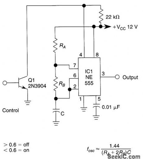
This gated 1-kHz oscillator offers press-to-turn-off' operation, A, and waveforms at the out-put of pin 3 and across C1, B. (View)
View full Circuit Diagram | Comments | Reading(1011)
SIMPLE_TIMED_TOUCH_SWITCH
Published:2009/6/24 21:06:00 Author:Jessie
This circuit produces an output for a time approximately equal to time constant R3/C1.
IC1,IC2 CD4011 quad NAND gateIC3 CD4066 quad bilateral switchC1 47-μF, 25-V electrolytic capacitorC2 100-μF, 25-V electrolytic capacitorC3 220-μF, 25-V electrolytic capacitorC4470-μF, 25-V electrolytic capacitorC5,C6,C7 0.1-μF capacitorRI,R3,R4,R6100-kΩ,1/4-W 5% resistorR7,R9,R10,R12 100-kΩ,1/4-W 5% resistorR2,R5,R8,R11 (View)
View full Circuit Diagram | Comments | Reading(1397)
GATED_1_kHz_OSCILLATOR(NORMALLY_OFF)
Published:2009/6/24 21:05:00 Author:Jessie
This gated 1-kHz oscillator offers press-to-turn-on operation, A, and waveforms at the out-put of pin3 and across C1, B. (View)
View full Circuit Diagram | Comments | Reading(996)
SIMPLE_TOUCH_SWITCH
Published:2009/6/24 21:05:00 Author:Jessie
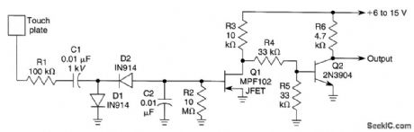
Q2 is held cut off since Q1 normally is conducting. When the touch plate is contacted by a large object (human body, etc.), stray 60-Hz pickup is rectified by D1 and D2, and produces a negative voltage across R2-C2 and the gate of Q1. Q1 cuts off, causes Q2 to conduct, and the output goes low. (View)
View full Circuit Diagram | Comments | Reading(1969)
TTL_OSCILLATOR_FOR_1_MHz_10_MHz
Published:2009/6/24 21:01:00 Author:Jessie
View full Circuit Diagram | Comments | Reading(1172)
96_MHz_CRYSTAL_OSCILLATOR
Published:2009/6/24 21:00:00 Author:Jessie
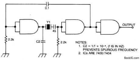
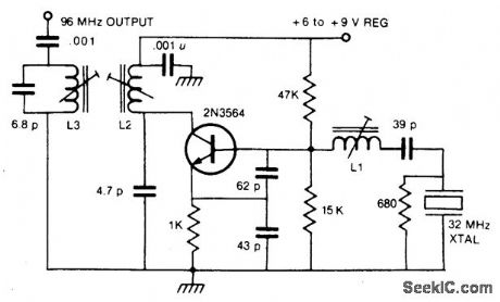
Circuit NotesBy usmg a crystal between 27.5 and 33 MHz,the 3rd harmonic will deliver between82.5 and 99 MHz. (View)
View full Circuit Diagram | Comments | Reading(1242)
| Pages:168/312 At 20161162163164165166167168169170171172173174175176177178179180Under 20 |
Circuit Categories
power supply circuit
Amplifier Circuit
Basic Circuit
LED and Light Circuit
Sensor Circuit
Signal Processing
Electrical Equipment Circuit
Control Circuit
Remote Control Circuit
A/D-D/A Converter Circuit
Audio Circuit
Measuring and Test Circuit
Communication Circuit
Computer-Related Circuit
555 Circuit
Automotive Circuit
Repairing Circuit