
Telephone-Related Circuit
Index 2
Circuit Diagram of adding visual judgment function to telephone ringing
Published:2011/8/9 18:18:00 Author:Vicky | Keyword: visual judgment function , telephone ringing
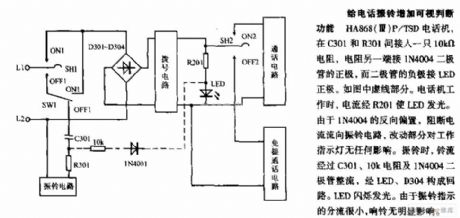
HA868(Ⅲ) P/ TSD telephone, adds a resistance of 10K Ω indirectly between C301 and R301, and connects the anode of diode IN4004 with the other side of the resistance while connects the cathode of the diode with the anode of LED. It is shown by dotted line in the picture. When the telephone works, the current goes through R201 and make the LED lighted. Because IN4004 is reversely biased, and prevents the current from flowing to ringing circuit, the revised part has no affection towards working indication light. When it starts ringing, the ring flows through C301, resistance of 10KΩ and diode IN4004, and becomes a loop via LED and D304. LED then twinkles and gives out light. Since the shunt of the ringing indication is very small, the ring is obviously affected. (View)
View full Circuit Diagram | Comments | Reading(1432)
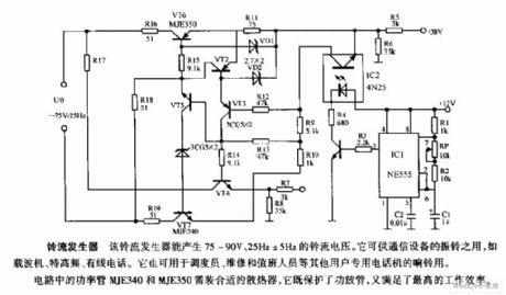
Ring current generator circuit diagram
Published:2011/8/9 18:20:00 Author:Vicky | Keyword: ring, current generator
Ring current generator
The ring current generator can produce a ringing current voltage of 75-90V and 25Hz±5HZ. It is available to be used for vibrating ring in communication devices, for example, carrier, ultrahigh frequency, wire telephone. It can also be used as ring in special telephone for dispatchers, repairmen, operators on duty and other users.
The power tube MJ3340 and MJE 350 in the circuit need suitable radiator to protect the power amplification tube and improve the work efficiency. (View)
View full Circuit Diagram | Comments | Reading(4706)
Circuit diagram of auto-adjustment for the telephone ring
Published:2011/8/9 18:22:00 Author:Vicky | Keyword: auto-adjustment , telephone ring
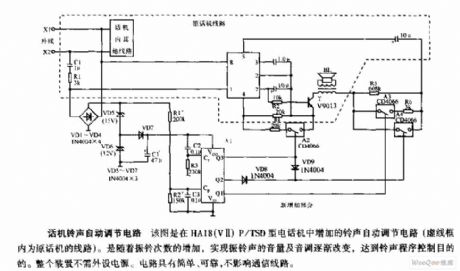
Auto-adjustment circuit of the telephone ring
The above picture is the auto-adjustment circuit added into the HA18(ⅤⅡ) P/ TSD type telephone (the circuit within the dotted frame is the original circuit of the telephone.). With the increasing numbers of the ring times, the gradual change of the ring volume and tone can be achieved and also the goal of control thr ringing procedure can be reached. The whole device needs no peripheral power supply. The circuit is simple and reliable. In addition , it does not affect the communication line. (View)
View full Circuit Diagram | Comments | Reading(1385)
Circuit diagram of constant-current-source type power supply and off-hook detection
Published:2011/8/9 18:23:00 Author:Vicky | Keyword: constant-current-source , power supply , off-hook detection
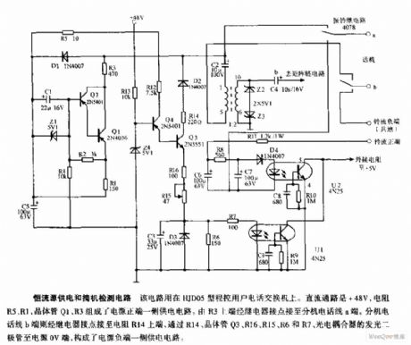
Circuit diagram of constant-current-source type power supply and off-hook detection
The circuit is used for HJD05 –type switching board. The direct current path is + 48V, and the resistances R5, R1, and the transistors Q1, Q3 constitutes a supply circuit in the positive end of the power supply. The upper end of R3 is connected with a end of the extension’s telephone line via a relay. The b end of the extension’s telephone line is connected to upper end of resistance R14 via a relay. The b end then is connected with 0V end of the power supply via R14, transistors Q3, R16, R15, R5, and R7, and the luminous diodes of the photoelectric coupler, which constitute the supply circuit in the negative end of the power supply. (View)
View full Circuit Diagram | Comments | Reading(3348)
Light-Operated Ring Circuit Diagram
Published:2011/8/9 18:24:00 Author:Vicky | Keyword: Light-Operated Ring
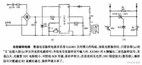
Light-Operated Ring Circuit
Average telephone ring circuit is composed of KA2401 and peripheral components. When adding light-operated ring circuit, just connects the part “X” in picture a with light-operated circuit in picture b. When there is input of AC ring signal into the exterior line, the pin 8 of KA2401 outputs ring signal of two tones. In the daytime, light sensitive tube 3DU has low resistance value, the SCR is conducted, and the volume of ring is relatively higher; in the evening, when there is no light, the resistance value of 3DU is very high (several megohms), the ring signal is weakened by R2 before passing through , so the volume of ring is much lower. (View)
View full Circuit Diagram | Comments | Reading(2045)
FM Wireless Microphone Circuit Diagram
Published:2011/8/9 18:01:00 Author:Vicky | Keyword: FM , Wireless Microphone
The following measures are taken to promise a clear voice of the microphone: the output signal of MIC is first sent to BG1 to be amplified. R1 and C1 is the additional pre-emphasized high-pitch sound circuit. C2 and C3 is the input and output coupling capacitance of tube BG1, the value of which is relatively lower to reduce the low-pitch sound and raise the mid and high sound. The diodes D3 and D4, which is connected in parallel in the BG1 output end , and the circuits C4 and C7, make use of the feature of the internal resistance ‘s being lower when the diodes are conducted in forward direction and influence the strong signal by limiting the amplitude. However, the regular signals remains unaffected. (View)
View full Circuit Diagram | Comments | Reading(3389)
TOUCH_TONE_DIALER
Published:2009/7/14 21:34:00 Author:May
Single Motorola 4410 chip requires only two external components and 2-of-8 keyboard to generate two sine waves simultaneously for Touch-Tone dialing and telephone modem communication. Each key on keyboard grounds one of C inputs and one of R inputs. As example, when 6 key is pressed, R2 and C3 are grounded to give 770-Hz sine wave on pin 2 and 1477-Hz sine wave on pin 15. Designed for driving 1K load. Output voltage is about 600 mV P-P for low output and 800 mV P-P for high output.-D. Lancaster, CMOS Cook-book, Howard W. Sams, Indianapolis, IN, 1977, p 132. (View)
View full Circuit Diagram | Comments | Reading(1342)
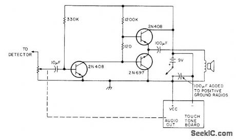
MOBILE_AUTOPATCH
Published:2009/7/14 21:12:00 Author:May

Circuit operates push-to-talk of mobile station automatically when any button on Touch-Tone pad is pushed for dialing telephone number after making auto patch, eliminating need for engaging microphone before dialing. Circuit remains active for about 2 s after Touch-Tone button is released.-Circuits, 73 Magazine, May 1977. p 19. (View)
View full Circuit Diagram | Comments | Reading(1397)
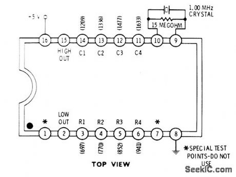
TONE_ENCODER
Published:2009/7/14 20:48:00 Author:May
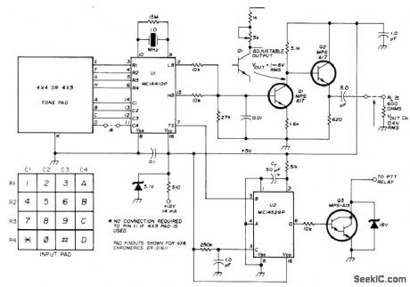
Motorola MC14410 CMOS IC is basis of accurate low-power Touch-Tone encoder system providing full 2-of-8 encoding from basic 1-MHz crystal oscillator. Can be used with 2-of-7 or 2-of-8 keypad switch matrix such as Chromerics ER-21623 or ER-21611. Q1-Q2 form tone-amplifiet/emitter-follower line driver. U2 is push-to-talk mono 1-s timer. Supply can be any voltage from 5to 12V if zener is used to supply 5 V to ICs. Article covers circuit operation in detail and gives tone-encoder frequency table.-J. DeLaune, Digital Touch-Tone Encoder for VHF FM, Ham Radio, April 1975, p 28-31.
(View)
View full Circuit Diagram | Comments | Reading(0)
TOUCH_TONE_ENCODER_1
Published:2009/7/14 20:36:00 Author:May
Consists of SME Touch-Tone generator and keyboard made by Data Signal (Albany, GA) mounted on any small transistor radio. Only audio section is used, with output tones from loudspeaker being fed acoustically to microphone of FM amateur station. Article gives construction details,-D. In-gram, The Shirt Pocket Touch-Tone, 73 Magazine, Nov. 1976, p 58-59. (View)
View full Circuit Diagram | Comments | Reading(1086)
BELL_SIMULATOR
Published:2009/7/14 6:08:00 Author:May

Uses AMI S2561 CMOS IC to simulate effects of telephone bell by producing tone signal that shifts between two predetermined frequencies at about 16 Hz. In applications where dial pulse rejection is not necessary, network inside dashed lines can be omitted and pins EN and D1 connected directly to VDD, which is typically 10V. Power is derived from telephone lines by diode-bridge supply. Values shown give tone frequencies of 512 and 640 Hz. Power output to 8-ohm loudspeaker is at least 50 mW, fed through 200:8 ohm trans-former.- Tone Ringer, American Microsystems, Santa Clara, CA, 1977, 52561, p 1. (View)
View full Circuit Diagram | Comments | Reading(1053)
TEMPERATURE_COMPENSATED_MILLIVOLT_REFERENCE
Published:2009/7/14 4:44:00 Author:May

Two identical diodes are used to derive a temperature -compensated voltage across R2. Select two diodes of the same manufacture with, for example, 10-mV difference in forward drop at the same current. Then the output will be compensated because both diodes will very likely have the same temperature coefficient (they are of identical manufacture). (View)
View full Circuit Diagram | Comments | Reading(1134)
TEMPERATURE_MONITOR
Published:2009/7/14 4:41:00 Author:May
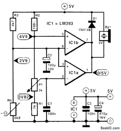
The temperature sensor is a resistor, R4, with negative temperature coefficient (NTC); the resistance of such a resistor drops when its temperature rises. Resistors R4 and R3 are part of a resistance bridge whose variable branch consists of R1, R2, and P1. The metering diagonal is connected to the inputs of comparator IC1a. The voltage at the inverting input of IC1a is set with P1 to a level that with normal temperatures is a little lower than that at the noninverting input. When the temperature rises, the resistance of R4 falls. This results in the comparator's changing state (to low), which causes the piezo buzzer to sound. Care should be taken to ensure that the voltage across the metering diagonal does not drop below 3.5 V to prevent the common-mode dynamic range of the LM393 from being exceeded. The NTC can be a 5- or a 10-kΩ type. It must be in good thermal con-tact with the heat source. Preset P1 must be set to a position where, after the part or device being monitored has attained normal operating temperature, the buzzer just does not sound. The buzzer must be a 5-V type. (View)
View full Circuit Diagram | Comments | Reading(0)
SOLID_STATE_THERMOMETER
Published:2009/7/14 4:38:00 Author:May
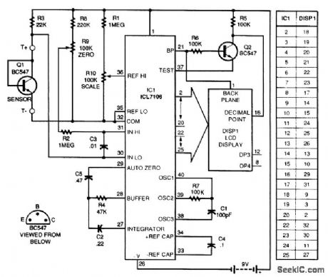
The AM ICL7106 31/2-digit analog-to-digital converter by Harris Semiconductor reads the -2.2-mV/°C change in the junction voltage drop of a BC547 transistor. R9 and R10 provide calibration. The basic chip has a 0- to 199.9-mV range. An LCD display made by Varitronix is used as a readout, The dc input voltage is correlated with the ambient temperature surrounding Q1. (View)
View full Circuit Diagram | Comments | Reading(3624)
PC_TEMPERATURE_INTERFACE
Published:2009/7/14 4:35:00 Author:May
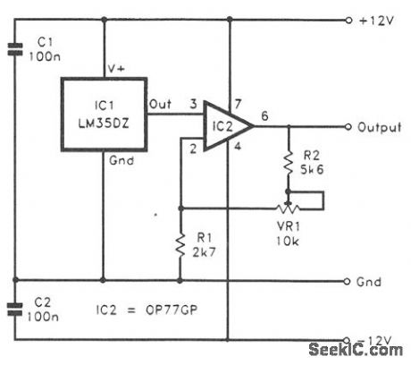
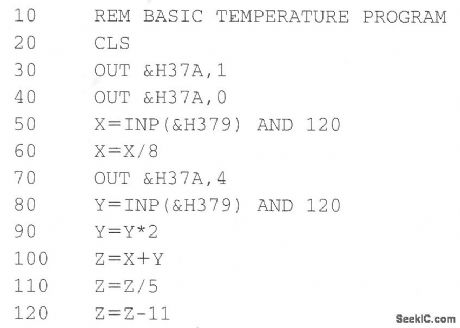
This simple temperature interface covers a range of 0 to 51°C. Dual balanced 12-V supplies were used to power the prototype, but dual 5-V supplies should just about suffice. IC1 is the temperature sensor. Over this range of temperatures, the LM35CZ should work well. The output from IC1 feeds into a noninverting-mode amplifier based on IC2. The closed-loop voltage gain of the amplifier is set by resistors R1 and R2 and preset VR1. The latter is adjusted to give a voltage gain of 5. VR1 is given the correct setting by first subjecting the sensor to a temperature, which is equal to about 50 or 100 percent of the full-scale value (i.e., about 20 to 51°C.). In most cases, the room temperature will be about 20 to 25°C, which will suffice. An accurate thermometer is used to measure the room temperature, and then VR1 is adjusted for the appropriate reading.
The following GW Basic or Q BASIC program reads the temperature sensor and prints the temperature on the screen: (View)
View full Circuit Diagram | Comments | Reading(1783)
LINEAR_READOUT_CIRCUIT
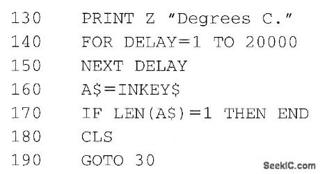
Published:2009/7/14 4:30:00 Author:May

Thermistors have found their way into a number of temperature-sensing applications. However, their resistance is a nonlinear function of temperature. In many applications, a digital readout of the thermistor also is desired. It is possible to produce a digital signal with a frequency that is linearly proportional to the temperature. The entire active portion of the circuitry can be implemented using 3/4 of an LM339. Comparator A is configured to operate as an op amp that generates voltage (Vt) which is inversely proportional to the thermistor's resistance, Rt. The voltage Vt is used as the thresh-old for the relation oscillator formed by comparators B and C. Comparator B monitors the voltage on the integrating capacitor (Vc). When it crosses Vt, it triggers the one-shot formed by comparator C via the signal Vtrig The output of comparator C resets the integrating capacitor for a duration, to, where to= (R2+3 kΩ)C2. Then the cycle begins again. The circuit achieves linear readout because the exponential nonlinearity of the thermistor is compensated by the exponential decay of the voltage in the relaxation oscillator. (View)
View full Circuit Diagram | Comments | Reading(1090)
TEMPERATURE_ADAPTER_FOR_DVM
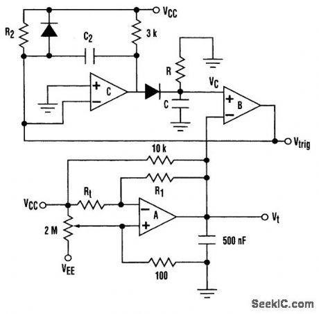
Published:2009/7/14 4:18:00 Author:May
A schematic for the temperature adapter is shown. The circuit outputs 0.01 V/°F. To determine temperature, you ignore the decimal point in the display, and the temperature readout is to the tenth of a degree. For example, if the temperature in a room is 75.5°, your DMM would read +0.755 V. The voltage input for op amp IC1 is obtained from a transistor Q1 used as a diode in this application. The linear voltage drop is measured and used to indicate temperature. The low-power regulator LM78L05 (IC2) provides a fixed 5-V source for the circuit. The voltage drop across Q1 is detected and amplified by IC1, an LM1458 op amp. The output of IC1 is then fed to the input terminals of a DMM. Put the positive lead of a voltmeter on pin 7 of IC1, and the negative lead on ground. Adjust R2 for a reading of 2.5 to 3 V. Connect the output of the adapter circuit to a voltmeter set to the 2-V dc scale. Adjust R8 so that the multimeter reads the same as a stabilized thermometer in the same vicinity as the temperature probe (ignore the decimal point). (View)
View full Circuit Diagram | Comments | Reading(1290)
TELEPHONE_LINE_SIMULATOR
Published:2009/7/14 3:23:00 Author:May

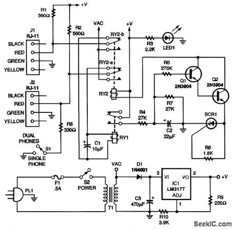
When both handsets are on-hook, resistors R1 and R2 supply power to them. When both hand-sets are off-hook, they transmit and receive their own audio. All the TCB does is supply power to them through R1 and R2. If switch S1 is closed, resistor R6 simulates a telephone being plugged into J2, permitting the testing of only one telephone. Now consider the situation where one handset is on-hook and one is off-hook. That causes the on-hook line to go to 24 Vdc and the off-hook line to go to 7 Vdc. The coil of relay RY1 is connected across the two telephone lines, and the voltage difference between the two lines energizes it. When the contacts of RY1 are closed, C2 charges through R4; it takes about 1 second for C2 to charge to 12 Vdc. The 12 Vdc across C2 causes a voltage-controlled switch consisting of R5, Q1, Q2, SCR1, and R8 to close, thus energizing RY2. When RY2 is energized, RY1 is removed from the circuit and a 60-Hz, 37-V p-p sine wave is placed on the telephone lines, causing the telephones to ring. Because RY1 is removed from the circuit, capacitor C2 starts discharging through R7. It takes about 1 second for the capacitor to discharge to about 2.4 Vdc. That lower voltage level causes the voltage-controlled switch to disable RY2, removing the ring voltage from the telephone lines and putting relay RY1 back in the circuit. If one telephone is still off-hook and one is on-hook, the cycle is repeated. (View)
View full Circuit Diagram | Comments | Reading(3466)
FM_TELEPHONE_TRANSMITTER
Published:2009/7/14 3:18:00 Author:May
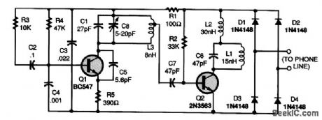
The circuit connects in series with either the tip or the ring (green or red) telephone line. Power for the circuit is full-wave bridge-rectified from the phone line by diodes Dl through D4. Transistor Q1, capacitors C1 and C8, and inductor L3 form an FM oscillator that operates at a frequency of around 93 MHz. Variable capacitor C8 allows the oscillator frequency to be adjusted between 90 and 95 MHz. To move the tuning area up to the 98- to 105-MHz range, C1 must be replaced with a 10-pF capacitor. Audio from the phone line is coupled through R3 and C2 to the base of Q1, where it frequency-modulates the oscillator. Transistor Q3, inductor L1, and capacitor C6 form a power amplifier. The signal tapped off L3 in the oscillator circuit is fed to the base of transistor Q2, and the FM signal is transmitted from Q2's collector. Inductor L2 is a radio-frequency shunt that decouples power and audio from the amplifier circuit. (View)
View full Circuit Diagram | Comments | Reading(150)
EMOTE_TELEPHONE_RINGER
Published:2009/7/14 3:09:00 Author:May
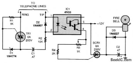
When there is no ring signal, the phone line's on-hook voltage (about 50 V) keeps the triac (Radio Shack 276-1001 or equivalent) from switching on, so the optocoupler doesn't conduct. When the phone rings, terminal 4 of the optocoupler feeds pulses through R3 and R4 to the gate of SCR1. The activated SCR connects the bell to the 12-V supply. Pulses are about 400 Hz, so the bell might sound a bit rough. The opening of the bell's breaker points cuts the thyristor's holding current to stop it from conducting when the gate signal stops. A 12-V, 2-A power supply operates the unit. Adjust R3 high enough so that the SCR is not triggered between rings, but low enough to trigger it when the phone is ringing. (View)
View full Circuit Diagram | Comments | Reading(2103)
| Pages:2/6 123456 |
Circuit Categories
power supply circuit
Amplifier Circuit
Basic Circuit
LED and Light Circuit
Sensor Circuit
Signal Processing
Electrical Equipment Circuit
Control Circuit
Remote Control Circuit
A/D-D/A Converter Circuit
Audio Circuit
Measuring and Test Circuit
Communication Circuit
Computer-Related Circuit
555 Circuit
Automotive Circuit
Repairing Circuit