
Circuit Diagram
Index 361
The output voltage increasing technology circuit with precision logarithmic and logarithmic ratio amplifier LOG102
Published:2012/8/28 2:53:00 Author:Ecco | Keyword: output voltage , increasing technology, precision, logarithmic , logarithmic ratio , amplifier
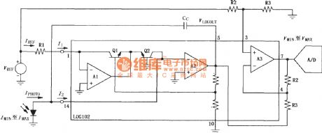
In many optical sensor detection applications, the output voltage increasing technology is just as important as increasing the photodiode current. In the Figure, the circuit uses a reference current generated by a large reference voltage source to adjust the error caused by LOG102 input offset voltage error to minimum; the reference current IREF flows into I1, the photodiode current IPHOTO flows into I2, IREF is designed to be greater than IPHOTO. The role of the internal amplifier A3 is to produce inverted gain level shift for calibration input photodiode current and corresponding the A / D converter input range.
(View)
View full Circuit Diagram | Comments | Reading(990)
Common-emitter amplifier circuit composed of double broadband transconductance operational amplifier OPA2662
Published:2012/8/28 2:44:00 Author:Ecco | Keyword: Common-emitter amplifier, double broadband , transconductance , operational amplifier
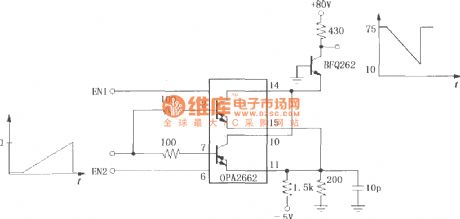
The circuit uses the OPA2662 internal dual OTA connected in parallel to constitute a common-emitter amplifier. The input end is connected 100Ω current limiting resistor in parallel, the input signal is input by 2 feet and 7 feet. 14 feet and 10 feet are connected the collector, 15 feet and 11 feet are connected to constitute the emitter, BFQ262 and 430Ω resistor form collector load, and the signal will be output after beng amplified, and the input and output waveforma are shown in Fig.
(View)
View full Circuit Diagram | Comments | Reading(831)
+12V single supply sampling instrument amplifier circuit with protective driver composed of SMP04 and instrument amplifier
Published:2012/8/28 2:39:00 Author:Ecco | Keyword: +12V, single supply , sampling instrument , amplifier , protective driver , instrument amplifier
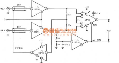
The circuit also uses the two channels of sample and hold amplifier SMP04 to constitute differential sampling with instrumentation amplifier AMP02. The signal is input (±) to SMP04, then it is differential amplified and output after being sampling and holding by AMP02. The other two sample-and-hold amplifiers' control terminal S / H are always grounded to keep the sample state. One is used to drive shielded cable to protect it from the interference from common-mode voltage; the other one is used to provide +6 V reference voltage for AMP02.
(View)
View full Circuit Diagram | Comments | Reading(1565)
Accurate peak-valley value detector circuit
Published:2012/8/28 2:13:00 Author:Ecco | Keyword: Accurate , peak-valley value , detector
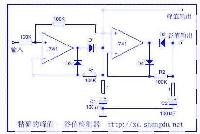
This circuit only uses two operational amplifiers to complete the peak-valley value detection of non-sine waveform. During the peak period, D1 breakover makes the C1 charge and reach peak, because of limiting effect of R1, C1 discharge minimal, charge again until the next peak to maintain the peak voltage output. Valley detection is contrary to the above values. C2 rapidly discharges to Valley value voltage by D2 during valley and trace discharges while other time only by D4, R2; C2 always remains valley voltage. The 1 Ω resistor connected to C1, C2 in series is used to prevent overshoot.
(View)
View full Circuit Diagram | Comments | Reading(3277)
HART-based protocol (highway addressable remote transducer communication protocols) smart transmitter with AD421
Published:2012/8/28 2:57:00 Author:Ecco | Keyword: HART-based protocol , highway, addressable , remote transducer, communication protocols, smart transmitter
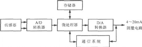
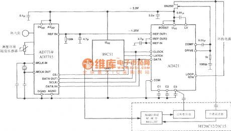
The frame and application diagrams of HART-based protocol smart transmitter with AD421 are shown as following:
(View)
View full Circuit Diagram | Comments | Reading(2330)
D/A converter (DAC) current loop interface circuit using multifunctional sensor signal conditioner AD694
Published:2012/8/28 1:35:00 Author:Ecco | Keyword: multifunctional sensor, signal conditioner , D/A converter , current loop , interface
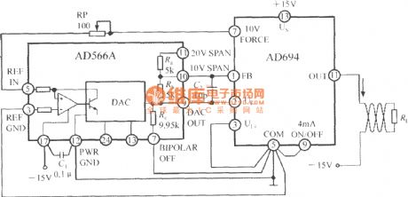
AD694 can be used as d/a converter (DAC) current loop interface to achieve the conversion of digital → voltage signal→ current signal . Current loop interface of DAC circuit is shown in the figure. AD566A is high speed 12-bit DAC, its output end (DAC OUT) connects to AD694 UI-end, UI+ end is grounded. AD694 uses ± 15V dual power supply, and AD566A provides reference voltage. AD694 uses the internal resistor network to configure AD566A as 10V full scale input. C2 is frequency compensation capacitor. RP is full scale adjustment potentiometer, you can use 50 Ω fixed resistors to replace potentiometer when it does not need adjustment.
(View)
View full Circuit Diagram | Comments | Reading(1910)
An experimental crystal oscillator FM transmitter circuit
Published:2012/8/27 22:46:00 Author:Ecco | Keyword: experimental , crystal oscillator , FM transmitter
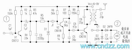
As shown in Figure 1, V1 and related resistive and capacitive components form the first level audio amplifier circuit which provides sufficient strength audio signals for modulating level. D1 is variable capacitance diode, and its equivalent capacitance varies with the reverse voltage on two poles, thus enabling center frequency of oscillator composed of crystal oscillator and external circuit change to achieve the purpose of FM. The signal output by oscillator is frequency doubled, amplified by the V3, then it is output by the tuned transformer after completing matching and filtering. The circuit uses tuned transformer, so it needs to restructure their cores after finished making. Its method is to produce a simple field strength circuit (as shown in Figure 2) to connect with the output terminal of the transformer, then adjusting the magnetic core until the ammeter indicating the maximum value.
(View)
View full Circuit Diagram | Comments | Reading(6626)
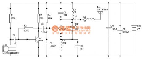
Simple long-distance wireless microphone circuit
Published:2012/8/27 21:45:00 Author:Ecco | Keyword: Simple, long-distance, wireless microphone
The loop antenna L1 for emission also serves as the oscillation coil, the high frequency current flowing in antenna has the same resonance with the oscillation frequency, so it is always in the best emission state. In practice, the launching distance is about 100-1850M in empty area ( receivers is a the Pocket Radio TOLY1781, and the receiver distance of antenna is added as 0.8m ), in contrast, under the equivalent working voltage, current and emission frequency, if L1 is changed by an ordinary spiral circle, oscillation transistor collector is connected to a 5PF capacitor with a 0 . 8M trolley line, the two launching transmission distances are almost equivalent to prove that the concealed shaped antenna, which is also used as the oscillator coil, has a quite high emission efficiency.
(View)
View full Circuit Diagram | Comments | Reading(3572)
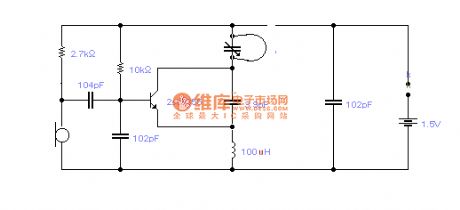
Simple FM transmitter circuit ( two tubes )
Published:2012/8/27 21:20:00 Author:Ecco | Keyword: Simple, FM transmitter , two tubes
View full Circuit Diagram | Comments | Reading(1856)
The stereo encoder circuit with discrete elements
Published:2012/8/27 22:15:00 Author:Ecco | Keyword: stereo encoder , discrete elements
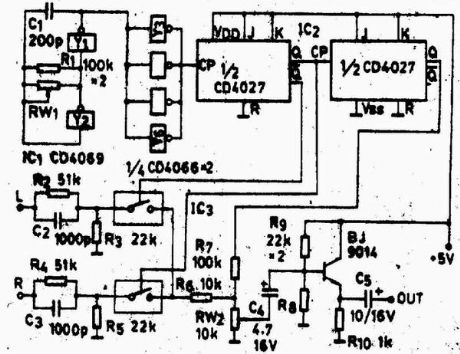
In the figure IC1-4069, Y1 and Y2 form a oscillator with frequency in 76KHZ; then the frequency is isolated and shaped by Y3-Y6 to be sent into frequency-halving circuit composed of IC2 and dual JK flip-flop CD4027, then it will produce a symmetrical + /-38KHZ and 19KHZ square wave, in which the + /-38KHZ square wave is used for controlling the IC3 analog switch CD4066; the stereo audio signal is input to switch for switching modulation, then it is mixed with 19KHZ frequency signal and sent to FM modulator after being isolated by the transistor 9014. FM modulator circuit can refer to a variety of FM transmitter circuits at the site.
(View)
View full Circuit Diagram | Comments | Reading(2148)
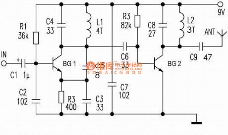
1000 m single-tube oscillation (C8050) FM transmitter circuit
Published:2012/8/27 22:27:00 Author:Ecco | Keyword: 1000 m , single-tube oscillation , FM transmitter
The circuit is very simple without debugging, you just need to make sure components are well connected without rosin joint and short circuit, it can work properly. Its power is about 60mw, so it is generally recommended to use rechargeable batteries which not only can provide large current, and be economy, and it is the ideal choice. But I do not advocate the transformer power supply, because it needs high filter circuit.
(View)
View full Circuit Diagram | Comments | Reading(2809)
The AD693 power consumption reducing circuit with a parallel external power tube
Published:2012/8/26 22:40:00 Author:Ecco | Keyword: power consumption reducing , parallel , external power tube
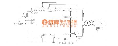
In the AD693, output transistor VT1 has the maximum power consumption, if necessary, it can use external power tubes connected in parallel to reduce their power consumption, the circuit is shown in the figure. VT2 can select 2N1711 or 2N2219A NPN power tube, its base connects to OUT-end, the collecting electrode connects to BOOST ends. It requires power tube's cutoff frequency fT=10~100MHz, AC current amplification coefficient β >10. 2N1711 and 2N2219A's main parameter: UCEO=75V, ICM=0.8A,PCM=0. 8W.
(View)
View full Circuit Diagram | Comments | Reading(1414)
Typical application circuit of the integrated current sensor MAX472
Published:2012/8/26 22:29:00 Author:Ecco | Keyword: Typical application , integrated current sensor
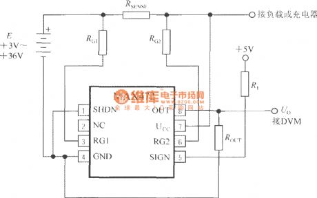
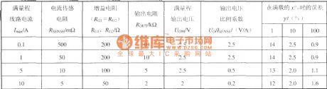
UCC termination is connected to load or charger, or power supply and battery pack. RG1 and RG2 are external gain resistors. R1, ROUT are respectively pull-up resistor and output resistor. With MAX472, the external component values can be selected according to the following table.
(View)
View full Circuit Diagram | Comments | Reading(1602)
PRTD signal conditioning circuit composed of multi-functional sensor signal conditioner AD693
Published:2012/8/27 1:38:00 Author:Ecco | Keyword: PRTD , signal conditioning , multi-functional sensor, signal conditioner
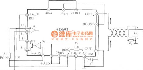
Platinum thermal resistor is a common temperature sensor, and there is a linear relationship between RT and temperature. AD693 has the the Pt100 platinum thermal resistance interface, which can be configured directly as PRTD signal conditioner, and the circuit is shown in Fig. Pt100's resistance value is 100Ω at 0℃, and the resistance change rate TCR = 0.00385Ω / Ω / ℃. The resistor can convert the temperature in range of 0 ~ +104 ℃ into 4 ~ 20mA current to complete temperature / current (T / I) conversion. The AD693 can set 6 different temperature ranges to meet the needs of different users.
(View)
View full Circuit Diagram | Comments | Reading(2204)
The accelerometer circuit with monolithic acceleration sensor MMA1220D
Published:2012/8/27 1:44:00 Author:Ecco | Keyword: accelerometer , monolithic acceleration sensor
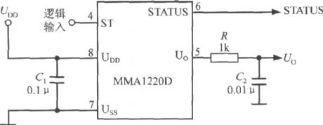
C1 is the power supply decoupling capacitor. R and C2 form a low-pass filter to filter out the switching capacitor to generate noise. Whenpin 4 inputs high, thechip reset.
(View)
View full Circuit Diagram | Comments | Reading(998)
Pipe pressure monitoring circuit with MPX4100A integrated Silicon pressure sensor
Published:2012/8/27 1:23:00 Author:Ecco | Keyword: Pipe pressure , monitoring circuit , integrated Silicon , pressure sensor
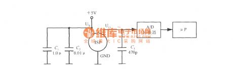
The typical application circuit of MPX4100A is shown in the figure, MPX4100A is used to monitor pipeline pressure. It uses the +5 V power supply, C1 and C2 are the power supply decoupling capacitors. C3 is the denoising capacitor of the output end. Integrated silicon pressure sensor output voltage (ISP) is first converted the digital by the A / D converter, and then sent to the microprocessor (μP) to calculate the measured pressure value. In order to simplify the circuit, it also can use microcontroller with A / D converter such as the Motorola company's MC68HC05 microcontroller.
(View)
View full Circuit Diagram | Comments | Reading(1136)
6 outputs circuit of integrated speed/voltage converter LM2907/2917
Published:2012/8/27 1:13:00 Author:Ecco | Keyword: 6 outputs , integrated , speed converter, voltage converter
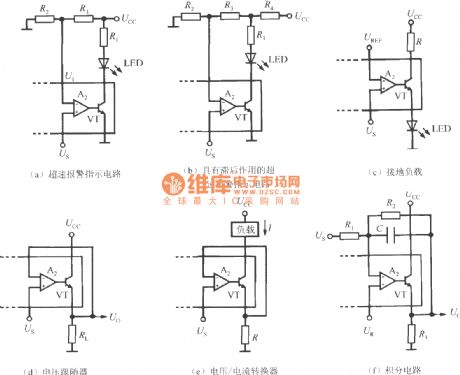
(a)Overspeed alarm indication circuit
(b)Overspeed alarm indication circuit with hysteresis
(c)Ground load
(d)Voltage follower
(e)Voltage/current converter
(f)Integrating circuit
(View)
View full Circuit Diagram | Comments | Reading(1563)
High-performance audio oscillator
Published:2012/8/27 1:02:00 Author:Ecco | Keyword: High-performance audio oscillator
View full Circuit Diagram | Comments | Reading(1223)
The current loop interface of D/A converter (1B22 isolated programmable voltage/current sensor)
Published:2012/8/26 21:46:00 Author:Ecco | Keyword: current loop , interface , D/A converter , isolated , programmable, voltage sensor, current sensor

The circuit can convert the analog voltage generated by D/A converter to isolated 4~20mA output current. D/A converter can use AD7245 (12-bit DAC) model, and its output voltage range is set to 0~10V. Using 1B22 can achieve circuit isolation and output over voltage protection.
(View)
View full Circuit Diagram | Comments | Reading(1848)
The brightness adjustment circuit with gated switch ( visible brightness sensor LX1970 )
Published:2012/8/26 22:08:00 Author:Ecco | Keyword: brightness adjustment , gated switch , visible , brightness sensor
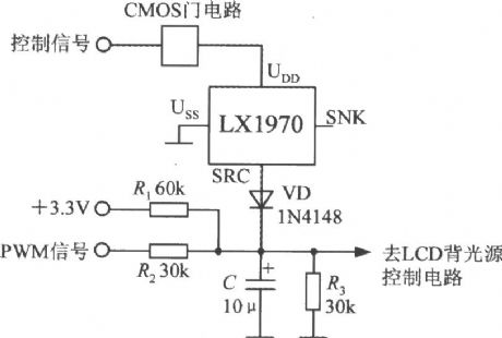
This circuit has the following characteristics: Firstly, it uses a CMOS gate circuit to control the power on-off of LX1970, only when the output of gate is high, LX1970 get electricity, LX1970 is a micro -power device, so the supply voltage can be provided by gate; Secondly, SRC end is connected to an isolation diode (VD ) in series, when LX1970 power down, VD is cut to play a role in isolation, the luminance signal can not be added to the LX1970; Thirdly, + 3.3V DC voltage signal and PWM signal can be equivalent to the two input signals of the logic oR gate, therefore, changing the DC voltage can also adjust the brightness. VD uses 1N4148 high-speed switching silicon diode.
(View)
View full Circuit Diagram | Comments | Reading(775)
| Pages:361/2234 At 20361362363364365366367368369370371372373374375376377378379380Under 20 |
Circuit Categories
power supply circuit
Amplifier Circuit
Basic Circuit
LED and Light Circuit
Sensor Circuit
Signal Processing
Electrical Equipment Circuit
Control Circuit
Remote Control Circuit
A/D-D/A Converter Circuit
Audio Circuit
Measuring and Test Circuit
Communication Circuit
Computer-Related Circuit
555 Circuit
Automotive Circuit
Repairing Circuit