
Circuit Diagram
Index 369
The bias zeroing circuit of logarithm and logarithmic ratio amplifier LOG100
Published:2012/8/13 21:43:00 Author:Ecco | Keyword: bias , zeroing circuit , logarithm, logarithmic, ratio amplifier
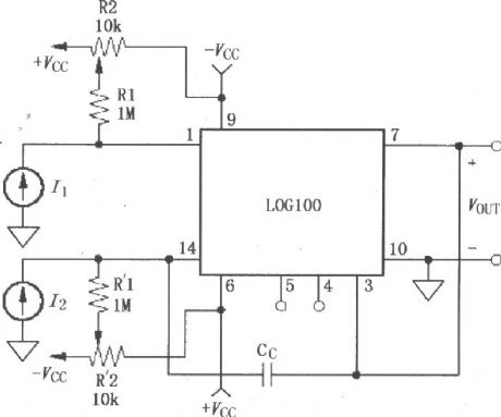
The circuit uses two 10kΩ potentiometers R2 , R2 to make zero set for input bias current ofinternal amplifiers A1, A2. Internal amplifiers A1 , A2are field effect transistor (FET) inputs, so the FET inputs havebias current feature which meansthe temperature increases 10 ℃, input bias current will be doubling. This bias zeroingcircuit can beonly used for the occasions with stable temperature.
(View)
View full Circuit Diagram | Comments | Reading(1185)
The current reverse input circuit of logarithm and logarithmic ratio amplifier LOG100
Published:2012/8/13 21:36:00 Author:Ecco | Keyword: current , reverse input , logarithm , logarithmic, ratio amplifier
LOG100's input current is positive current, andit means usually the input current can only flow to pin 1 and pin 14. In some applications, the signal current is negative current , such as photomultiplier tubes. The circuit can solve this problem, which uses the circuit in the attached diagramto convertnegative signal current to positivecurrent inflowing toLOG100.
(View)
View full Circuit Diagram | Comments | Reading(1155)
Common base (common -B) amplifier circuit of broadband transconductance operational amplifier and buffer OPA660
Published:2012/8/13 22:06:00 Author:Ecco | Keyword: Common base, common -B, amplifier , broadband , transconductance , operational amplifier, buffer
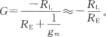
Figure (a) shows the discrete components common-base amplifier , Vo is the in-phase gain, Vos has a few volts; figure ( b ) shows the common-base amplifier composed of OPA660. Vo is the inverting gain , Vos = 0V.
(View)
View full Circuit Diagram | Comments | Reading(1391)
General application circuit diagram of three-terminal adjustable output regulator
Published:2012/8/12 21:08:00 Author:Ecco | Keyword: General application , three-terminal , adjustable output , regulator
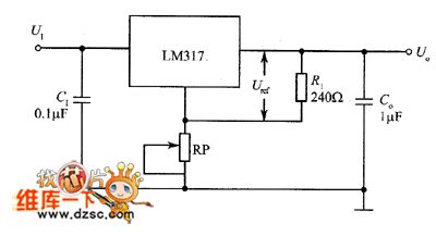
Figure 1 shows the general application circuitof three-terminal adjustable positive output integrated voltage regulator circuit ( adjustable negative output voltage regulator has a similar circuit). In the circuit, R1 and RP form the resistor network with adjustable output. in order to makebias current and the tube's leakage currentbe absorbed, R1 is set in the range of 120 ~ 240Ω .The discharge currentflowing throughR1 is 5 ~ 10mA. The input capacitor C1 is used to suppress the ripple voltage. The output capacitor C is used to eliminate vibration andbuffer the impact of load to guarantee the stability of the circuit operation.
(View)
View full Circuit Diagram | Comments | Reading(949)
Current feedback amplifier circuit of broadband transconductance operational amplifier and buffer OPA660
Published:2012/8/13 22:03:00 Author:Ecco | Keyword: Current feedback , amplifier, broadband , transconductance, operational amplifier , buffer
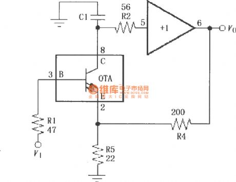
Signal V1 is input to pin 3 of OPA660 by 47Ω resistor and output from pin 6 after being amplified by the internal +1 amplifier; at the same time, pin 2 of OPA660 gets feedback from pin 6 by 200Ω resistor to constitute the current feedback amplifier. The current feedback amplifier can be used to stabilize static operating point, expand broadband and reduce the output distortion of amplifier. Circuit gain G = 1 + R4/R5 = 10.
(View)
View full Circuit Diagram | Comments | Reading(1574)
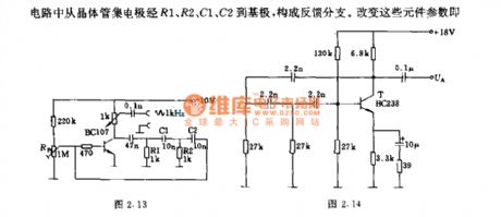
The capacitive lag compensation circuit composed of LF398
Published:2012/8/13 22:15:00 Author:Ecco | Keyword: capacitive lag compensation
C1, R1 , R2 andR3 constitute a capacitance lag compensation circuit,and the time constant C1 = τ/100kΩ; adjusting potentiometer R3 can adjust the output amplitude.
(View)
View full Circuit Diagram | Comments | Reading(1667)
The basic circuit diagram of mirror constant current source
Published:2012/8/12 20:52:00 Author:Ecco | Keyword: basic circuit , mirror , constant current source
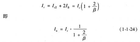
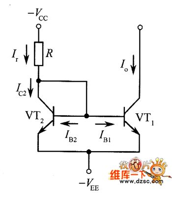
The basic circuit of the mirror constant current source is shown as the figure,and VT1, VT2 are MAPs. From the figure, the Ir = Ic2 + IB1 + IB2. Because VT1, VT2are symmetrical, the collector currentis equal tobase current, so
When Ir is determined, the constant current source output current Io is also identified. When β is large enough , Io ≈ Ir, and that is, the output current is approximately equal to the reference current , the circuit is often referred to a current mirror circuit.
(View)
View full Circuit Diagram | Comments | Reading(1650)
Direct-reading LC meter circuit
Published:2012/8/13 22:23:00 Author:Ecco | Keyword: Direct-reading , LC meter
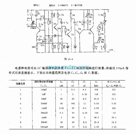
Inductor and capacitor can be tested by the circuit composed of LC oscillator and transistors T1 ~~ T5, and displayed directly by 100μA pointer instrument. The following table shows the measurement range and values of capacitors C0 , CL , L0 and f0.
(View)
View full Circuit Diagram | Comments | Reading(2355)
Simple regulator tester circuit
Published:2012/8/13 22:37:00 Author:Ecco | Keyword: regulator , tester

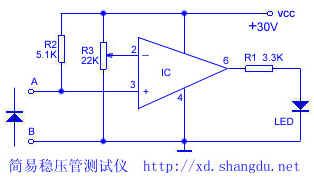
Simple regulator tester circuit can easily test the value of regulator, and its production is very convenient.
The schematic is shown as the following figure. ICcan select F007, CA3140, μA741 amplifiers, R3 Selects 22K straight sliding potentiometer,and the voltage should be marked on the shell according toaccording to the positive supply voltage required by R3. In addition , due to the limitations of the IC operating voltage, the lcircuit is imited to the measure theregulator tube with valuebeing lower than30V.
(View)
View full Circuit Diagram | Comments | Reading(1168)
Junction field effect transistor matching test circuit
Published:2012/8/13 22:41:00 Author:Ecco | Keyword: Junction , field effect transistor, matching test circuit
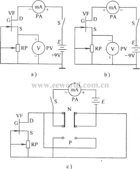
Figure a shows the circuit which can test matchingN-channel junction field effect transistor tube. Figure b shows the circuit which can test the matchingP-channel junction field effect transistor tube . Figure a shows the circuit which can testmatching N, P junction field effect transistor tube.
(View)
View full Circuit Diagram | Comments | Reading(1908)
High-power transistors test circuit with multimeter
Published:2012/8/13 22:47:00 Author:Ecco | Keyword: High-power transistors, multimeter, test circuit
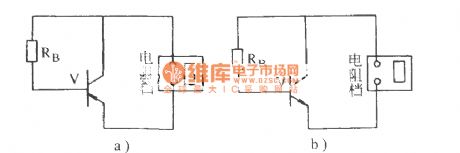
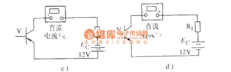
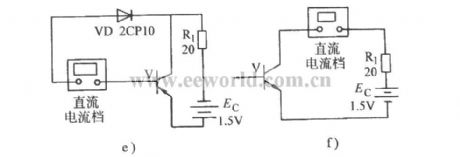
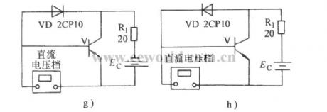

Figure a, bare used to testthe amplification of high-power transistor . Figure c, dare used to testthe Iceo of high-power transistors. Figure E, fare used tothe hFE of high-power tube. Figure g, hare used to test high-power transistor UB . Figure i, kare used totest high-power transistors UBES and UCES.
(View)
View full Circuit Diagram | Comments | Reading(1817)
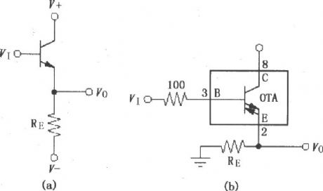
Common emitter (common -E) amplifier circuit of broadband transconductance operational amplifier and buffer OPA660
Published:2012/8/13 22:09:00 Author:Ecco | Keyword: Common emitter , common -E, amplifier , broadband , transconductance, operational amplifier , buffer
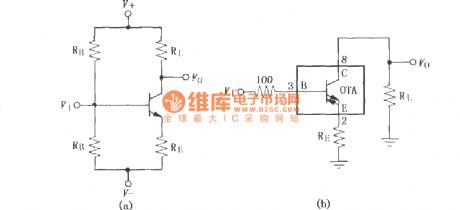
Figure (a) shows the discrete componentscommon- emitter amplifier, andtransconductance changes in the whole temperature range , Vo is the inverting gain , Vos only has a few volts. Figure (b) shows common emitter amplifier composed of the OPA660, andthe transconductance is a constant in the whole temperature range, Vo is the in-phase gain , Vos = 0V.
(View)
View full Circuit Diagram | Comments | Reading(768)
Simple sinusoidal oscillator
Published:2012/8/13 20:56:00 Author:Ecco | Keyword: sinusoidal oscillator
The oscillation signal is adjusted by the potentiometer Rp1. The output resistor is low ( 1kΩ ), so it is applied to a variety of control circuits for the signal source. In the circuit, the transistor collector through R1 , R2, , C1, , C2 to the base and constitutes the feedback branch. Changing the parameters of these components can change the frequency range.
(View)
View full Circuit Diagram | Comments | Reading(1113)
Digital 440MBit / s sending system driver amplifier circuit composed of OPA2662
Published:2012/8/13 21:53:00 Author:Ecco | Keyword: Digital , 440MBit / s , sending system , driver , amplifier
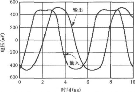
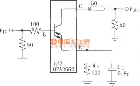
Input and output impulse response waveforms are shown as below. The cicuit uses an OTA which is inside of OPA2662 to constitute a common-emitter amplifier, that is, the input -end is added 100Ω current limiting resistor and 50Ω matching resistor, then the signal is amplified and output to drive 50Ω cable and load. Io = ± 17mA.
(View)
View full Circuit Diagram | Comments | Reading(775)
Common collector (common -C) amplifier circuit of broadband transconductance operational amplifier and buffer OPA660
Published:2012/8/13 22:11:00 Author:Ecco | Keyword: Common collector , common -C, amplifier , broadband , transconductance , operational amplifier, buffer
G=1. Figure (a) shows the discrete components common-collector amplifier , Vos = 0.7V ; Figure ( b ) shows common-collector amplifier ( buffer ) composed of OPA660, Vos, = 0V.
(View)
View full Circuit Diagram | Comments | Reading(1272)
Simple single field-effect transistor oscillator circuit
Published:2012/8/12 22:19:00 Author:Ecco | Keyword: Simple , single , field-effect transistor , oscillator
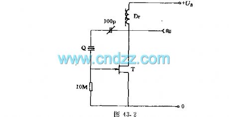
This circuit uses a field-effect transistor to constitute a quartz crystal oscillator circuit with excellent performance, the tuning capacitor is used to adjust the scope, and choke can be selected according to the frequency range to make WL be greater than 20kΩ.
(View)
View full Circuit Diagram | Comments | Reading(1671)
100MHz power oscillator circuit using dual- gate FET
Published:2012/8/12 22:35:00 Author:Ecco | Keyword: 100MHz , power oscillator , dual- gate , FET
The oscillator uses tuning resonant circuit as the working resistor of the FET. Oscillating power signal is output by the fast switching transistors T1 and T2.
(View)
View full Circuit Diagram | Comments | Reading(2323)
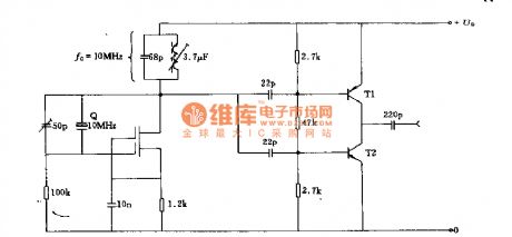
Crystal quartz crystal oscillator circuit using FET
Published:2012/8/12 22:41:00 Author:Ecco | Keyword: Crystal , quartz , crystal , oscillator , FET
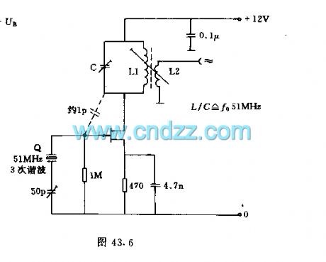
Crystal oscillator works as 51MHz crystal( the third harmonic of 17MHz) . According to the different structures, the drain - gate capacitance can be selected between 0.5 to 1.8 pF. L2's turns are about 20% of the L1. 470 Ω source resistor can change the oscillation characteristics.
(View)
View full Circuit Diagram | Comments | Reading(1929)
Grating circuits using integrated circuit
Published:2012/8/14 3:16:00 Author:Ecco | Keyword: Grating circuits, integrated circuit
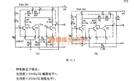
This circuit uses TAA293 as a threshold switch. 1KΩ resistor is used to adjust the value of the photoresistor and threshold of threshold switch. Two circuits are suitable for the occasions: the light intensity is greater than 1000lx ( Q end is in high level) , light intensity is less than 300lx ( Q end is in low level).
(View)
View full Circuit Diagram | Comments | Reading(781)
TA7240AP internal block diagram and its main parameters
Published:2012/8/11 1:51:00 Author:Ecco | Keyword: internal block , parameters
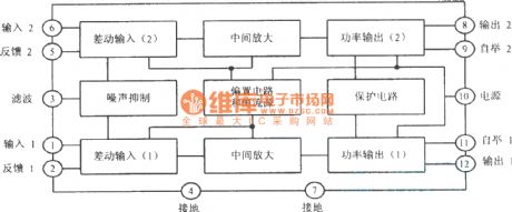
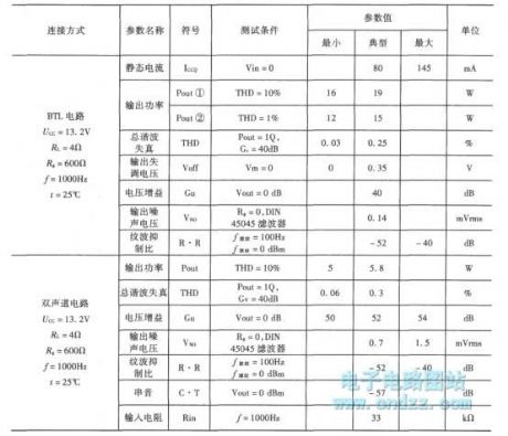
TA7240AP is thestereo audio power amplifier IC produced by Japan's Toshiba Corp. It has high-fidelity, low-noise , high-power characteristics.It iswidely used in early audio equipments.
Its main parameters can be seen at the following table:
(View)
View full Circuit Diagram | Comments | Reading(1201)
| Pages:369/2234 At 20361362363364365366367368369370371372373374375376377378379380Under 20 |
Circuit Categories
power supply circuit
Amplifier Circuit
Basic Circuit
LED and Light Circuit
Sensor Circuit
Signal Processing
Electrical Equipment Circuit
Control Circuit
Remote Control Circuit
A/D-D/A Converter Circuit
Audio Circuit
Measuring and Test Circuit
Communication Circuit
Computer-Related Circuit
555 Circuit
Automotive Circuit
Repairing Circuit