
Circuit Diagram
Index 373
High-power Darlington internal circuit diagram
Published:2012/7/8 21:55:00 Author:Ecco | Keyword: High-power Darlington
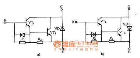
Ordinary Darlington's DC magnification hFE is particularly high, so it is used normally only below 2W. When the power increases, the tube's pressure drop make temperature increase, pre- transistor leakage current will be gradually enlarged, resulting in the deterioration of the overall thermal stability. In order to overcome this deficiency, the high-power Darlington is set balanced resistor, and it is also connectrd a freewheel diode VD between C and E reverse to make over-voltage protection. When the inductive load ( relay coil ) is suddenly cut off, VD can release the reverse voltage to prevent the breakdown of the internal transistor. Figure a shows the internal circuit of high-power PNP Darlington, and Figure b shows the internal circuit of NPN type high-power Darlington.
(View)
View full Circuit Diagram | Comments | Reading(1184)
Transistor radio tuning instruction circuit diagram
Published:2012/7/5 20:37:00 Author:Ecco | Keyword: Transistor radio, tuning instructions
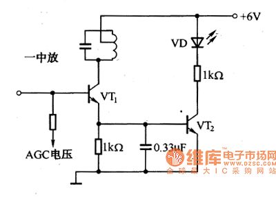
The transistor radio tuning instruction circuit is shown in Figure 1 . When the tuner is accurate, the AGC voltage is minimum, and the emitter current of VT1 is minimum, and emitter voltage drop is also minimum, VT2's emitter current is minimum, then the light emitted by light-emitting diode VD is darkest; conversely, if the tuning is offset, light-emitting diode's light is enhanced. So it can be accurately tuned according to this characteristic.
(View)
View full Circuit Diagram | Comments | Reading(2429)
Pulse discrimination circuit diagram
Published:2012/7/5 21:02:00 Author:Ecco | Keyword: Pulse discrimination
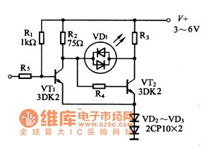
Figure 1 is a pulse discrimination circuit diagram composed of color light-emitting diodes. When the positive pulse arrives , VT1 is breakover, then color light - emitting diode VD1 emits green light; VT2 is breakover when there's no pulse, the color light-emitting diode VD1 emits red light . And people can distinguish the presence or absence of pulse according to this.
(View)
View full Circuit Diagram | Comments | Reading(932)
Isolated converter circuit diagram composed of LT1425
Published:2012/7/3 22:29:00 Author:Ecco | Keyword: Isolated converter
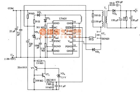
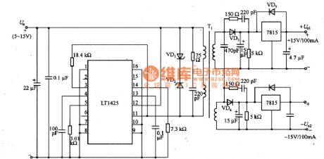
Figure a, b are the isolated converter circuit composed of LT1425. The input voltage of the circuit shown in Figure (a) is -36 ~-72V, and the output is 5V/2A. The LT1425 is an integrated circuit with current working way, and the oscillation frequency is 275kHZ. It has all the features required by the power supply circuit, and the leakage current of the on-chip switching power MOSFET is 1.5A . The circuit does not impose feedback, so the load adjustment rate is ± 5% . In order to increase the stability of the load changes and remove a part of voltage from the output to add to the feedback side, people enhancethe stability of the circuit.
Figure (b) is a dual-output converter circuit using LT1425. The circuit has no a negative feedback circuit, its output is added a three-terminal integrated regulator 7815 to increase stability. When the input voltage is 5V, the conversion efficiency is 72% ; when the input voltage is 15V, the conversion efficiency is 80% , and its isolation performance depends on the structure of the winding of transformer T1.
(View)
View full Circuit Diagram | Comments | Reading(1936)
Current resonance converter circuit diagram composed of NE555
Published:2012/7/3 22:13:00 Author:Ecco | Keyword: Current resonance converter
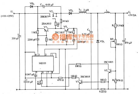
Figure 21 shows the current resonance converter circuit diagram composed of NE555. In the circuit, NE555 is the voltage controlled oscillator. MOSFET (VT1 ), freewheeling diode VD2 and smoothing inductor L1 constitute a common step-down DC / DC converter. L2 and C1 form the resonant circuit, VD2 is a diode to realize half-wave current resonance. VD1 and C3 form the bootstrap circuit to provide gate drive current for the the VT1. Voltage divider resistors R1 , R2 and RP1 are used to detect the output voltage, and the voltage is added to the VT5's base to control the frequency of the NE555. VT3 is the overcurrent protection circuit which can control the output current in the range of 0.5 ~ 3A.
(View)
View full Circuit Diagram | Comments | Reading(3131)
Regulated power supply application circuit diagram
Published:2012/7/3 21:42:00 Author:Ecco | Keyword: Regulated power supply , application
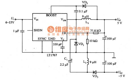
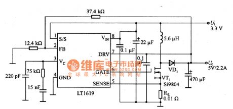
Figure a, b show the application circuits of LT1619 and LT1767. Figure (a) is the application circuit of the LT1619. It is the current controller, and it can be used as step-up inductive single-ended converter and flyback converter when the external components is rare. LTl619's external components is rara, which has small size with high efficiency. LTl619 can converter the input voltage of 3.3V to 5V/2.2A output. Under heavy load, the conversion efficiency is higher than the other converters, and the voltage on the current sense resistor drops to only 5OmV with samll resistor power loss, resulting in improved conversion efficiency. When the load is light, it works with burst way to maintain high conversion efficiency. The typical operating frequency is 300kHz. When it is in synchronization with external clock, the operating frequency can get 5OOkHZ. No-load current is 14OμA, while standby current is only 15μA.
(View)
View full Circuit Diagram | Comments | Reading(1524)
The amplifier circuit diagram composed of M5106P
Published:2012/7/3 22:06:00 Author:Ecco | Keyword: amplifier
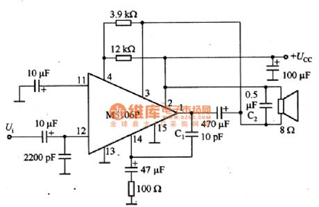
Figure 4-42 shows the amplifier circuit composed of M5106P. The circuit can be used as main power amplifier with output power in 1W. As the M5106P has no zero end, it is very easy to use. In order to make the circuit operation stably, you should note the following : pin 13 and pin 15 are grounded to the input end, and pin 1 and pin 14 should access phase compensation capacitor C1 to prevent the oscillating capacitance from connecting 8Ω speaker load. When the supply voltage is 9V , the output power is 1W; when the power supply voltage is 6V, it only can receive 0.5W output.
(View)
View full Circuit Diagram | Comments | Reading(2278)
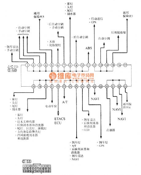
The Southeast Soveran relay connector ( J / C ) electrical system circuit diagram
Published:2012/7/2 3:50:00 Author:Ecco | Keyword: Southeast Soveran, relay connector , electrical system

View full Circuit Diagram | Comments | Reading(965)
Basic inverting integrator circuit diagram
Published:2012/7/1 20:19:00 Author:Ecco | Keyword: inverting integrator
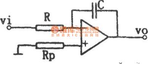
The integrator circuit consists of operational amplifiers and resistors, capacitors. The operational amplifier incircuit can be selectedaccording to the computing precision, but the circuit 's output voltage and current should not exceed the rated output value of the op amp, Vom and Iom.
(View)
View full Circuit Diagram | Comments | Reading(898)
SN75490 thermal print head driver circuit diagram
Published:2012/7/1 20:35:00 Author:Ecco | Keyword: thermal, print head driver
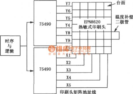
SN75490 is used to drive many commonly used thermal print head, and it contains six AND gate drivers with common strobe pulse. Each driver has a totem pole output, and the calibration output voltage range is 4.75 ~ 3.5V, input side is compatible with TTL and 5V CMOS, and the power supply current capacity is 30mA . Absorption current capacity is 50mA, and the standard supply voltage is ±5V, it has strobe input end.
(View)
View full Circuit Diagram | Comments | Reading(2363)
The integrator (LM318) circuit diagram with expanded timing range
Published:2012/7/1 20:27:00 Author:Ecco | Keyword: integrator, expanded timing range
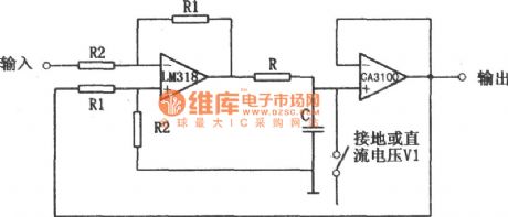
The integrator can easily work with a very short and very long time constant. The integration time constant is ( R2/R1) RC , if the precision of resistors R1 , R2 is ± 0.1 % , you can get a very good linearity . The advantages of this circuit are: it is easy to adjust its initial state because the capacitor is grounded with one end. If the switch is grounded at one end, the output is zero when switch is closed, the initial state is zero ; If one end of switch is connected to voltage V1, the initial state is V1. The integration period of the circuit can be as short as 1ns or as long as 1000s. The bandwidth of the integrator depends on the characteristics of the op amp. The integrator composed of LM318 and CA3100 op amps is suitable for high frequency signal points.
(View)
View full Circuit Diagram | Comments | Reading(1773)
60h timing circuit
Published:2011/12/1 21:39:00 Author:May | Keyword: 60h timing
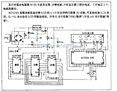
This timer consists of three parts: power supply double 50Hz square wave generator, frequency dividing circuit, timing display. Its working volt is 5V. Its current is several milliampere.
5G7224A is 4 1/2 bit fully decoded counter driving LCD. It is 60 system and it can direct-coupling LCD. D1~D5 state each bit LCD drive line group. Switch K is used for controlling time/suspend ; Switch AN is used for controlling zero clearing .
(View)
View full Circuit Diagram | Comments | Reading(1839)
5kHz electric eye oscillation circuit
Published:2011/12/1 21:27:00 Author:May | Keyword: 5kHz, electric eye, oscillation
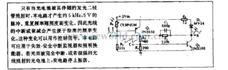
This circuit can generate 5kHz, 5V pulse only when electric eye is shined by its incidental LED. Repeat frequency changes along with illumination intensity. So the break off or weaken of optical line can generate frequency variation. This frequency variation is easy to detect. It can be usedfor controlling signal. This circuit can be applied to invalidation-safe interrupt monitor and illumination transducer. If the beam isinterrupted completely, or very strong optical line shines on electric eye, the circuit stops oscillation.
(View)
View full Circuit Diagram | Comments | Reading(1650)
BQ2000 charge controller
Published:2011/12/1 21:23:00 Author:May | Keyword: charge controller
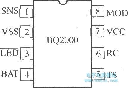
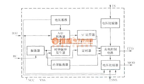
BQ2000 charge controller is pioneer product currently inpower source technology field. It intergrates each element circuit charge controller needed in one IC. The arithmetic unit in the chip can make the whole circuit control be more precise, operation bemore safe, function be more complete. Its pin array is shown in the following diagram.
The internal functional block diagram is shown in the following diagram:
(View)
View full Circuit Diagram | Comments | Reading(2013)
DS2762 pin array diagram
Published:2011/12/2 0:33:00 Author:May | Keyword: land patten
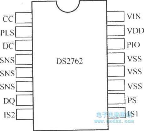
DS2762 is lithium ion battery monitor chip. It is produced by Maxin company. It can real-time monitor the parameter of voltage, current, charge and discharge condition and dump energy, etc. The chip can store this data. The chip can provide this data to SCM. And SCM can do relvant treat to the data. DS2762 chip cancollect data, store information. DS2762 chip hasthe features of functional integrity, external wiring simple and so on. Its pin array is shown in the following diagram.
(View)
View full Circuit Diagram | Comments | Reading(1543)
DS2438 used for measuring traction battery packs circuit
Published:2011/12/2 1:21:00 Author:May | Keyword: traction battery packs, measuring
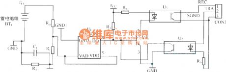
Traction battery packs test chip produced by America Dallas company has rich function, and itis convenient to achieve monitoring the running state of electric motor car’s traction battery packs.
DS2438 can beused for monitoring of various kinds of traction battery packs. The utility power used in electric motor car is traction battery packs composed of multiple power battery connecyed in series, parallel. The performance of each power battery directly affectsthe characteristic of whole traction battery packs. So in practical application, we should make on-line real-time detection to each power battery. And each power battery should connectwith a piece of DS2438, and their data terminal can be articulated to a bus. The power supply source of DS2438 can come from tested power battery itself. The potential of DS2438 signal end DQ is to the ground of this DS2438. The potential of reference ground is different, so it must cause the difference of potential of DS2438 signal end DQ inthe same reference point. It is shown in the diagram.
(View)
View full Circuit Diagram | Comments | Reading(1721)
Single chip switching power supply design
Published:2011/11/13 21:59:00 Author:May | Keyword: Single chip, switching, power supply, design
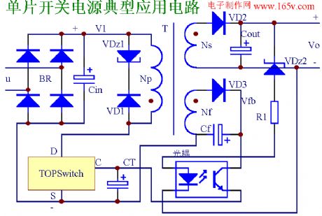
The typical application circuit of TOPSwitch series single chip switching power supply is shown in the diagram. High-frequency transformer in the circuit has three functions of energy storage, isolation output and voltage transformation. The diagram shows thatthe polarity of high frequency transformer primary winding Np is coincided with the opposite polarity of secondary winding Ns and the feedback winding NF. This indicates that the electrical energy is stored in the primary winding in the type of magnetic energy when TOPSwitch is broken over, and meanwhile VD2 is closed. When TOPSwitch is cut off, VD2 is broken over, energy will transfers to the secondary, namely, it is the features of fly-back switching power supply. In the diagram, BR is the rectifier bridge; Cin is the input end offilter capacitor. AC voltage u is rectified and filtered and then it will get DC high voltage V1. After passing the primary windings, it will add to the drain of TOPSwitch. In view of the TOPSwitch cut-off time, the spike voltage generated by drain of high frequency transformer can be superimposed on the DC high voltage V1 and the induced voltage Vor. It can make the brain voltage of power switching tube exceed 700V and damage the chip. So it must increase drain clamping protection circuit in the justified of primary winding. (View)
View full Circuit Diagram | Comments | Reading(3082)
Small switching power supply module using TOP222P
Published:2011/11/13 21:34:00 Author:May | Keyword: Small switching, power supply
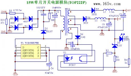

AC input voltage is 100~245V, double way DC output (note 1), the biggest output is separately 10V800mA, 5V800mA, and the power supply efficiency is 80%~89%. ( note 1: whenthe output is5V, this power supply module has the function of regulation voltage) (View)
View full Circuit Diagram | Comments | Reading(4835)
34063 used for DC-DC supply convert circuit
Published:2011/12/1 20:17:00 Author:May | Keyword: DC-DC supply convert
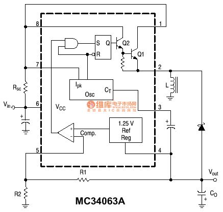
34063 is a kind of intergrated circuit which is used for DC-DC power supply converter.It canbeused for voltage boost, step-down and polarity reversed. The highest polarity reversed effect is 90%, the highest step-down effect is 80%, conversion efficiency and work frequency filter capacitorare indirect proportion. Moreover, when output power can not reach therequired value, for example, when >250~300MA, it can enlarge current through the method of external expansion power tube, andambipolar or MOS expansion current tube is ok.The peripheral cell nominal meaning and their value computing formula:Vout (output value)=1.25V(1+R1/R2)Ct (timing capacitor):decide internal operating frequency. Ct=0.000004*Ton (work frequency)Ipk=2*Iomx*T/offRsc (current-limiting resistance):decide output current. Rsc=0.33/IpkLmin(inductance): Lmin=(Vimin-Vces)*Ton/IpkCo ( filter capacitor): decide output voltage ripple factor, Co=Io*ton/Vp-p(ripple factor)fixed value parameter:Vces=1.0V ton/toff=(Vo+Vf-Vimin)/(Vimin-Vces) Vimin: minimum value when input voltage unsteadinessVf=1.2V high-speed switch diode forward voltage drop (View)
View full Circuit Diagram | Comments | Reading(2193)
The combination sine wave circuit of 400Hz LED and operational amplifier
Published:2011/11/10 0:09:00 Author:May | Keyword: sine wave, LED, operational amplifier, 400Hz
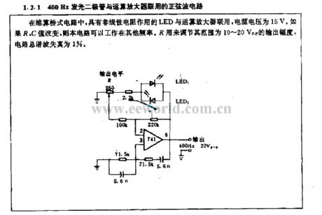
In dimensional calculation bridge circuit, LED with norlinear resistor usage and operational amplifier are used in combination, and the power supply voltage is 15V. If R,C values change, this circuit can work at other frequency. R can adjust output width and its range is 10~20Vp-p, and the circuit total harmonic distortion is 1%.
(View)
View full Circuit Diagram | Comments | Reading(1627)
| Pages:373/2234 At 20361362363364365366367368369370371372373374375376377378379380Under 20 |
Circuit Categories
power supply circuit
Amplifier Circuit
Basic Circuit
LED and Light Circuit
Sensor Circuit
Signal Processing
Electrical Equipment Circuit
Control Circuit
Remote Control Circuit
A/D-D/A Converter Circuit
Audio Circuit
Measuring and Test Circuit
Communication Circuit
Computer-Related Circuit
555 Circuit
Automotive Circuit
Repairing Circuit