
Circuit Diagram
Index 364
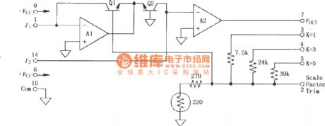
Voltage buffer circuit with twice of output current composed of broadband transconductance op amp and buffer OPA660
Published:2012/8/22 22:18:00 Author:Ecco | Keyword: Voltage buffer , twice , output current, broadband transconductance , op amp , buffer
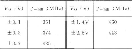
The essence of this circuit common collector ( total -C) amplifier circuit of OPA660, and it uses a common collector (Total -C) amplifier circuit's current amplification effects to set the resistor of OTA in figure and current gain in 2, then to form a voltage buffer with twice of output current. Parameter settings are shown in the table below.
(View)
View full Circuit Diagram | Comments | Reading(999)
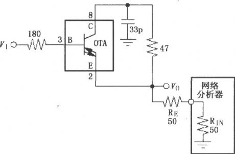
Logarithmic function-transformation circuit with negative input current I1 ( logarithmic amplifier 4127)
Published:2012/8/22 21:42:00 Author:Ecco | Keyword: Logarithmic, function-transformation circuit, negative input current, I1 , logarithmic amplifier
As shown in the figure, the circuit is logarithmic function-transformation circuit when thesignal I1is input asvoltage form and I1 is a negative. When the input I1 is added to pin 7 of 4127 with negative direction, the output voltage Eo=-A•log(|I1|/ IR), then output is transformed to logarithmic form.
(View)
View full Circuit Diagram | Comments | Reading(754)
Single-end input, double-end output differential line driver circuit composed of OPA2662
Published:2012/8/22 22:24:00 Author:Ecco | Keyword: Single-end input, double-end output, differential, line driver
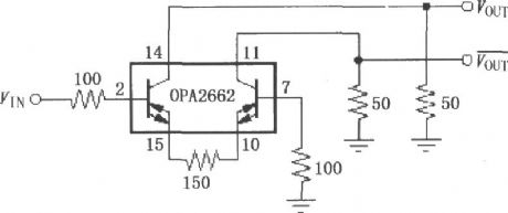
It usestwo identical amplifiers contained in dual op amp OPA2662 to form the circuit shown in Figure, OTA2's inputend -pin 7 is grounded by 100 resistor, OTA1 input end -pin 2 is the input end,and the single-end input signal VIN is amplified by pin 14 and and output pin 11.
(View)
View full Circuit Diagram | Comments | Reading(1846)
1600 × 1200 high-resolution graphics monitor CRT output stage driver circuit composed of OPA2662
Published:2012/8/22 22:28:00 Author:Ecco | Keyword: 1600 × 1200 , high-resolution , graphics monitor, CRT, output stage, driver

The circuit utilizes OPA2662's internal two OTAs to constitute a common-emitter amplifier, that is, input end is added 150Ω current limiting resistor and 50Ω termination resistor, and the signal is amplifed to pass CR3425 and drive CRT monitor. At the input end, , tR = 0.7 ns , tF = 0.7 ns ; , tR = 2.4ns , tF = 2.15ns.
(View)
View full Circuit Diagram | Comments | Reading(975)
Logarithmic function-transformation circuit with negative input voltage E1 ( logarithmic amplifier 4127)
Published:2012/8/22 21:22:00 Author:Ecco | Keyword: Logarithmic, function-transformation circuit , negative input voltage, E1, logarithmic amplifier
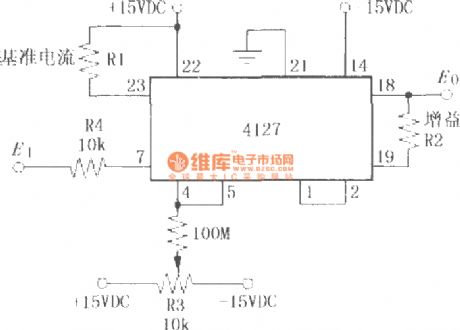
As shown in the figure, the circuit is logarithmic function-transformation circuit when thesignal E1is input asvoltage form and E1 is a negative. When the input E1 is added to pin 7 of 4127 with negative direction, the output voltage Eo=-A•log(|E1|/R4 • IR), then output is transformed to logarithmic form.
(View)
View full Circuit Diagram | Comments | Reading(1696)
Drift zeroing circuit of logarithmic and logarithmic ratio amplifier LOG101/104
Published:2012/8/22 21:02:00 Author:Ecco | Keyword: Drift zeroing , logarithmic , logarithmic ratio , amplifier
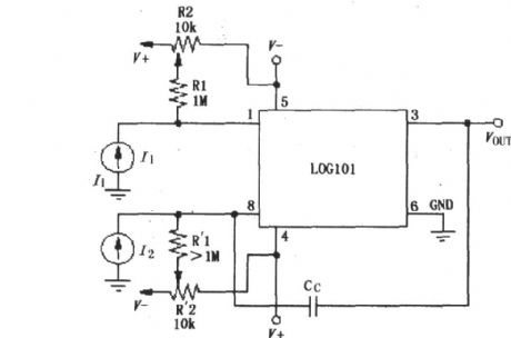
LOG101/104 input current I1/I2 is limited in the range of 100pA ~ 3.5mA, and if input current is greater than 3.5mA, the nonlinearly will be increased; if input current is less than 100pA, the input bias current ( typical value 5pA) will cause the input error to increase. When ± 5V supply operates, the input current (I1 + I2) is limited to 4.5mA. The circuit uses two 10kΩ potentiometers R2, R'2 to zero the input bias current of internal amplifiers A1 , A2. The internal amplifiers A1 , A2 control the field - effect transistor (FET) input, so the FET input has bias current characteristics, and temperature increases to 10 ℃ will double the input bias current.
(View)
View full Circuit Diagram | Comments | Reading(810)
Basic signal and power connection circuit of logarithmic and logarithmic ratio amplifier LOG101/104
Published:2012/8/22 21:11:00 Author:Ecco | Keyword: Basic, signal , power, connection , logarithmic, logarithmic ratio , amplifier
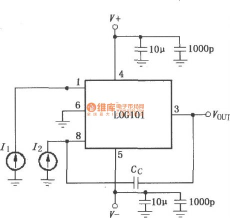
Signal current I1/I2 is input to pin 1 and pin 8, then pin 3 outputs voltage VOUT = (1V) · log (I1/I2). In order to reduce the impact of the wire inductance, positive and negative supply terminal must be added to decoupling capacitor, and 10μF tantalum capacitor and 1000pF ceramic capacitor are connected in parallel to constitute a decoupling capacitor, and 1000pF ceramic dielectric capacitor is mainly used to filter out high frequency noise.
(View)
View full Circuit Diagram | Comments | Reading(958)
Single supply +5 V operating circuit of logarithmic and logarithmic ratio amplifier LOG101/104
Published:2012/8/22 20:50:00 Author:Ecco | Keyword: Single supply , +5 V , operating circuit , logarithmic , logarithmic ratio , amplifier
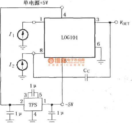
Many applications only have a single power supply, while LOG101/104 needs dual power. The circuit shown in figure uses a negative pump power TPS6040DBV which can switch a single +5 V power supply to a -5V supply for LOG101/104.
(View)
View full Circuit Diagram | Comments | Reading(946)
4127 logarithmic amplifier
Published:2012/8/22 20:44:00 Author:Ecco | Keyword: logarithmic amplifier
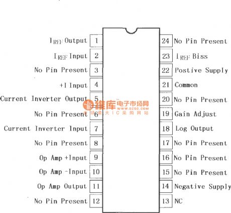
4127 is the first hybrid logarithmic amplifier with double width DIP ceramic package, it can accept either polarity signal from the current source or voltage source. 4127 is the ASIC chip for logarithmic transformation with accurate 6 decimal input current and 4 decimal input voltage. In addition, a current inverter and an internal precision reference make pin programmable to complete the functions of logarithmic, logarithmic ratio and antilog amplifier. In order to further increase its versatility and reduce the cost of the user's system, the internal 4127 encapsulates an operational amplifier which can be used as a buffer, filter or gain elements. The initial accuracy of 4127 is 0.5% and 1.0%, and it can work in ambient temperature range of -10 ~ +70 ℃. The 4127 versatility and high performance have many uses, such as signal compression, sensor linearization, light electrical buffer, as well as in the manufacturing of medical devices, analytical instrumentation and process control instruments.
(View)
View full Circuit Diagram | Comments | Reading(2397)
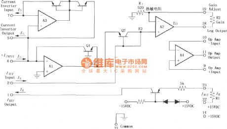
Harmonic generator circuit
Published:2012/8/22 20:33:00 Author:Ecco | Keyword: Harmonic generator
The harmonics generator composed by the two comparators and a summing amplifier is shown in Fig 11-20. It can use any non- square wave including sine, triangle, sawtooth waveform to get harmonic, and harmonic is widely used in phase-locked loop, waveform generator, electronic musical instruments and other harmonic applications. When the comparator is input a harmonic, it will produce an output pulse, the width is proportional to the sum of input amplitude and reference voltage. Changing the reference voltage can allow the pulse width to change between from 0 to 100 %. The harmonic spectrum changes with pulse width, you can use the duty cycle to determine the offset harmonic.
(View)
View full Circuit Diagram | Comments | Reading(1255)
Low frequency oscillator circuit with TcA580
Published:2012/8/22 20:18:00 Author:Ecco | Keyword: Low frequency , oscillator
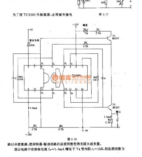

In order to use TCA580 as oscillator, the circuit must connect an external circuit for attenuation, then the loop - oscillation loop's quality factor becomes infinite or negative. In the circuit shown as the figure, when emitter current IE =1.6mA, internal resistance of T4 tube re= 16Ω.
(View)
View full Circuit Diagram | Comments | Reading(1469)
A variety of sound effects generator circuit
Published:2012/8/21 22:18:00 Author:Ecco | Keyword: variety , sound effects , generator
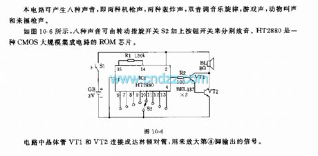
This circuit can produce eight kind of sounds, namely two kinds of machine gunfire, two kinds of bomb sound, dual tone music melody, game sound, animal calls and the sound of rifle shot. As shown in figure 10-6, eight kinds of sound can be played respectively by switching rotary switch S2 and pushing button switch. HT2880 is a kind of CMOS large-scale ROM chip. The transistors VT1 and VT2 in circuit are connected as Darlington pipe which is used to amplify the signal output from pin 4.
(View)
View full Circuit Diagram | Comments | Reading(1413)
Rain sound generator circuit
Published:2012/8/21 22:43:00 Author:Ecco | Keyword: Rain sound generator
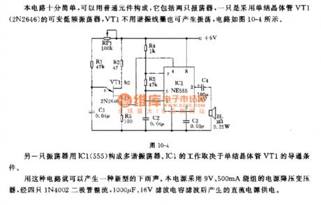
The circuit is very simple, and it is composed of common elements, it includes two oscillators: one is a variable low frequency oscillator which uses single-junction transistor VT1 (2N2646), VT1 can generate oscillation circuit without resonant coil, the circuit is shown in Figure 10-4. The other oscillator and IC1 (555) constitute a multivibrator. IC1 work depends on the conduction conditions of the single-junction transistor VT1. This circuit can produce a new type of rain sound. The power supply uses 9V, 500mA winding power step-down transformer, and the power is rectified by four 1N4002 diode, filtered by 1000μF and 16V filter capacitor to become DC power supply.
(View)
View full Circuit Diagram | Comments | Reading(1682)
Ultra-low frequency multivibrator
Published:2012/8/21 22:46:00 Author:Ecco | Keyword: Ultra-low frequency , multivibrator
View full Circuit Diagram | Comments | Reading(767)
Precision logarithmic and logarithmic ratio amplifier LOG100
Published:2012/8/21 22:57:00 Author:Ecco | Keyword: Precision logarithmic , logarithmic ratio , amplifier
LOG100 uses advanced integrated circuit technology to achieve its high accuracy, and it is easy to use with low cost and small size to make logical logarithmic arithmetic. The maximum error of amplifier in specifications ensure is more than 6 decimal input range (1nA ~ 1mA) and all possible I1 and I2 combinations. As to ensure the total error, it does not require the calculation of the concerned error. The circuit uses a special design which is compatible with film monolithic integrated circuit, including amplifiers, logarithmic transistors and low drift thin-film resistors. In order to guarantee maximum precision, the thin film resistor uses laser correction.
(View)
View full Circuit Diagram | Comments | Reading(973)
The lc wobbulator circuit with varactor diode
Published:2012/8/21 21:27:00 Author:Ecco | Keyword: lc wobbulator , varactor diode
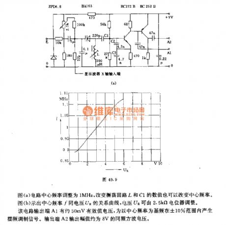
Figure (a) shows the circuit with center frequency being adjusted to 1MHz, center frequency can also be changed by the oscillation circuit L and the value of C1.Figure (b) shows the curve between the center frequency f and voltage UR, voltage UR can be adjusted by 2.5kΩ potentiometer.The circuit output terminal A1 has about 50mV RMS voltage, the center frequency will generate modulated signal in the he baseband pendulum frequency range of ± 10%. The output terminal A2 has the same frequency square wave voltage with 8V output amplitude.
(View)
View full Circuit Diagram | Comments | Reading(2184)
Pulse keying ring oscillator
Published:2012/8/21 22:08:00 Author:Ecco | Keyword: Pulse, keying, ring , oscillator
View full Circuit Diagram | Comments | Reading(1450)
Ultrasonic Insect Killer
Published:2012/8/21 21:31:00 Author:Ecco | Keyword: Ultrasonic Insect Killer
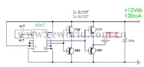
This is a very simple ultrasonic mosquito, insects, cockroaches repellercircuit.The circuit is a relaxation oscillation circuit which iscomposed of the CMOS 4047 monoflop, adjusting 4K7 can makeits center frequencybe approximately 22KHz, four transistors form bridge power output to promote the 3.25 inch Piezo and emit ultrasonic signals.
(View)
View full Circuit Diagram | Comments | Reading(4256)
Gate voltage generator circuit
Published:2012/8/21 22:01:00 Author:Ecco | Keyword: Gate voltage generator
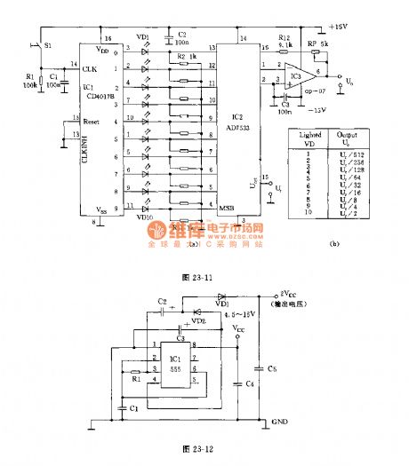
FET is commonly used in low-power instruments. When it works, the gate voltage should be higher than the source voltage 9V, it is inconvenient to use battery-powered low-voltage circuit.Working principle: the circuit is shown in Figure 23-12. This circuit can provide high gate voltage. 555 oscillator drives a voltage multiplier to produce the output voltage which is twice of the input voltage. Generally FET ignores gate current, the output current of circuit is very small, and it can provide gate voltage to the 10 FETs without voltage drop at the same time.
(View)
View full Circuit Diagram | Comments | Reading(1098)
The circuit of 100kHz oscillator
Published:2012/8/21 3:40:00 Author:Ecco | Keyword: 100kHz oscillator

The circuit uses a standard quartz crystal oscillator SQ4804A, and the bias between output frequency and standard frequency does not exceed 100 × 10-6. The oscillator control the following amplifier (BC108) to output square wave, and it uses the integral circuit to obtain up to 8 branches of output, then to control the eight gates.
(View)
View full Circuit Diagram | Comments | Reading(2584)
| Pages:364/2234 At 20361362363364365366367368369370371372373374375376377378379380Under 20 |
Circuit Categories
power supply circuit
Amplifier Circuit
Basic Circuit
LED and Light Circuit
Sensor Circuit
Signal Processing
Electrical Equipment Circuit
Control Circuit
Remote Control Circuit
A/D-D/A Converter Circuit
Audio Circuit
Measuring and Test Circuit
Communication Circuit
Computer-Related Circuit
555 Circuit
Automotive Circuit
Repairing Circuit