
Circuit Diagram
Index 377
Projector lamps thyristor AC regulating voltage circuit
Published:2011/8/29 1:13:00 Author:Jessie | Keyword: Projector lamps, thyristor, AC regulating voltage
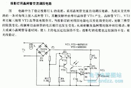
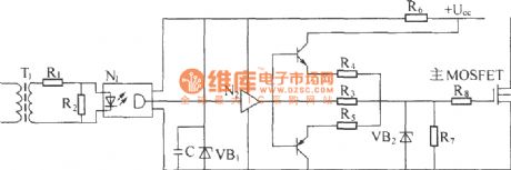
In order to steady projector lamps L's brightness, it uses thyristor AC regulating voltage circuit. So that it adds thyristor T5 to the AC bridge road. It's triggering pulse is produced by unijunction transistor VT4. The transistors VT1, VT2 and light activated triode VT3 has the same function. When projector lamps' light changing with power voltage's change,light activated triode's value changes, and the voltage phase which controls unijunction transistor changes too, so that the pulse triggering transistor's phase moves to increase or decreae the transistor conduction time, L voltage approximate remain, the brightness of the projector lamps also approximate remain, then the light keeps stability.
(View)
View full Circuit Diagram | Comments | Reading(1897)
DHY29-[48]24/10 type DC-DC converter principle diagram
Published:2011/12/4 22:04:00 Author:May | Keyword: DC-DC converter
![DHY29-[48]24/10 type DC-DC converter principle diagram](/uploadfile/ic-circuit/s2011410204646624.jpg)
At present, most communication equipments arealready unified and standard to use 48V DC power supply. But there are also few equipments continue using 24V DC power supply. Because the needed capacity of current is small, if we use rectifier toprovide power, for the purpose of guarantee incessant energy supply, we must use 24V accumulator battery. It is clear that it is not economy and occupation the space of equipment room. The suitable method to solve this problem is adopting 48V to 24V DC-DC converter. The diagram is DHY29-[48]24/10 type DC-DC converter principle diagram, its main performance index:
(1) input DC voltage nominal value: 48V permit change range: 41V~51V
(2) output DC voltage nominal value: 24V/10A permit change range: 21.6V~26.4V
(3) precision of voltage regulation: ≤±1%
(4) noise voltage phone balance weight noise voltage: ≤2mV, broadband noise voltage: ≤20mV (3.4kHz~30kHz) , peak to peak value noise voltage: ≤100mV, discrete frequency: ≤5mV (3.4kHz~150kHz) ≤3mV (150kHz~200kHz) ≤2mV (200kHz~500kHz) ≤1mV (0.5MHz~30MHz)
(5) efficiency: ≥80%
(6) Over voltage, under voltage, over current protection point and cut-off current. Over current: (29±1) V, under voltage: (21±1)V, over current: (12±1)V, cut-off current:10.5A~11A
(7) The current equalization of parallel operation: ≤±5% (View)
View full Circuit Diagram | Comments | Reading(1344)
Low-power AC-DC universal motor thyristor control circuit
Published:2011/8/29 1:08:00 Author:Jessie | Keyword: Low-power , AC-DC universal motor , thyristor control
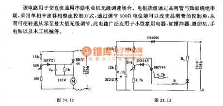
This circuit is used inAC/DC general motor thyristor speed adjustment occasions. The armature winding series isconnected to excitation winding, single-phase half wave phase shifting rectifier, and adjusting500Ω potentiometer can change thyristor's control Angle, so that speed is adjusted from 0 to maximum. This circuit is widely used in small household appliances such as blenders, sewing machines, hand drills and woodworking machinery.
(View)
View full Circuit Diagram | Comments | Reading(2468)
AC/DC general motors no hysteresis adjustable violations circuit
Published:2011/8/29 0:57:00 Author:Jessie | Keyword: AC/DC general motors, adjustable violations
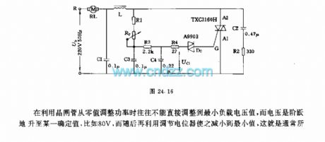
When ituses thyristor to cotrol power,theminimum load voltage always can't be directly from 0 , but voltage is stepped to a fixed value, for example, 80V can be reduced to the minimum valueby adjusting potentiometer, this is commonly said hysteresis effect. This circuit makes AC/DC general motors driving 300W, and adjusting potentiometer Rp can adjust the speed of motor.
(View)
View full Circuit Diagram | Comments | Reading(1041)
Two normal shock converter circuit principle diagram
Published:2011/12/4 21:49:00 Author:May | Keyword: Two normal shock, converter
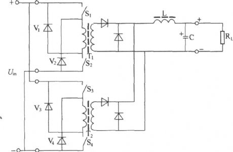
When it needs high output power, we always adopts two transistors forward converter circuit with superimposed voltage, and it isshown in the diagram. The features of the circuit:
(1)two normal shock converting circuits are connected inparallel, T1 and T2 are driven in 180opposite phase, then the power increases one time, and output frequency adds one time, ripples and dynamic responseare improving;
(2) S1, S2 are connected in series (S3, S4 are connected in series) , then the pressure-proof of switching tube is decreasd inhalve;
(3)The circuit cancels feedback coils, V1, V2, VpV4are energy recovery routes, it decreases the request of transformer’s manufacture craft.
(4)It hasthedead area limiting feature, two parts do nothave the problem of common circulation, its reliability is high. (View)
View full Circuit Diagram | Comments | Reading(1392)
Intermittent oscillator control thyristor circuit
Published:2011/8/29 0:52:00 Author:Jessie | Keyword: Intermittent oscillator, thyristor
We can use intermittent oscillator T2 to control the anti parallel thyristor circuit, the width of its oscillation pulse is40 μs, pulse frequency is 3kHz. Switch S opens theoscillator, thyristor is always triggeredwhen the positive half cycle begins. In fact, the function of switch S can be taken by transistor T1.
(View)
View full Circuit Diagram | Comments | Reading(1643)
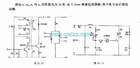
Electromagnetism thyristor control circuit
Published:2011/8/29 0:51:00 Author:Jessie | Keyword: Electromagnetism, thyristor
The vibration electromagnet in blender is general supplied by AC 220V. In order to makemixing, the electromagnet's pendulum pictureis often required uneven, it can be produced by former meet resistance's double half wave circuit. but the thyristor circuit controlled by phase shifting can avoidthe loss from resistance. The main technical parameters of circuit are: Working voltage: 220 ~ 380V; Working current: maximum 6A; The positive half cycle phase shifting range: 0 ~ 180 °.
(View)
View full Circuit Diagram | Comments | Reading(1323)
Series photoelectric couplers control thyristor switch circuit
Published:2011/8/29 0:48:00 Author:Jessie | Keyword: Series photoelectric couplers, thyristor switch
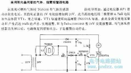
When the combustible gas appears, TGS308 gas sensor's conductivity increases,and thevoltagepassing potentiometer RP1's sliding point increases from normal 3V RMS to 20V. This increased voltage added to transistor VT1 makes2N6070A connect. The waveAC voltage driver H produces 90dB sounds torealize alarm. H is Delta16003168 24V AC alarm.After gases disappears from the sensor, circuit recoverys original state, so alarm automatically stops.
(View)
View full Circuit Diagram | Comments | Reading(794)
The driver circuit of switching power supply
Published:2011/12/4 21:35:00 Author:May | Keyword: driver, switching power supply
Driver circuit principle diagram:
Driver circuit of switching power supply:
The main function of driver circuit is enlarge the variable width pulse output by pulse width controller forthe driver signal of high voltage power supply switching device. Driver circuit generally has theisolatingfunction. It always uses transformer coupling mode to energizethe high voltage power switching device and isolate input stage and output stage. Meanwhile it can add reverse bias when power switching device is cut off to increase the speed of cut-off device. When it drives MOSFET devices, the common driver circuit is achieved by a driver transformer. (View)
View full Circuit Diagram | Comments | Reading(1050)
Below 3kw electromagnetic valve non-contact bi-directional thyristor connect circuit
Published:2011/8/29 0:41:00 Author:Jessie | Keyword: electromagnetic valve, non-contact, bi-directional thyristor
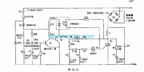
When the switchgets the power, light-emitting diode LD52 is connected. The photoconductor FW9802 which accessed to bi-directional thyristor'sdoor loop is decreased to 2.5kΩ, and it makes the loop's current enoughfor trigger thyristor's conduction, electromagnetic valve power supply. After 5s, RC charging circuit makes T1 connect, T2 cut off, light-emitting diode current interrupt, and then photoconductor's value increase, thyristor shut off, electromagnetic valve blackout.
(View)
View full Circuit Diagram | Comments | Reading(1399)
Bi-directional thyristor circuit with Flip-flop TCA780
Published:2011/8/28 22:52:00 Author:Jessie | Keyword: Bi-directional thyristor, Flip-flop
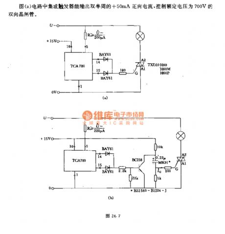
In figure a, integrated flip-flop can output double half cycle +50mA positive current to control the Bi-directional with 700 V rated voltage. Figure b is the reverse controlled current circuit. +15V Power supplycharges for0.22 μF capacitor through 10kΩ resistor, and the chanrging polarity is shown as the chart, then the transistor BC238 stops. When the pulse generated by the integrated trigger is added to the base of transistor by passing two diodes, the transistor is turned on, then the capacitor is grounded by the transistor, so the gate pole on thyristor generates a reverse trigger current to turn it on.
(View)
View full Circuit Diagram | Comments | Reading(1736)
Low resistance power distribution circuit
Published:2011/4/11 2:18:00 Author:may | Keyword: Low resistance, power distribution
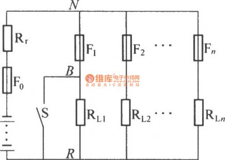
The diagram is low resistance power distribution circuit, among, R is battery internal resistance, RL1~RLn is load of each branch path; F1~Fn is safety wire of each branch path; F0 is battery safety wire, up and down two bold lines state total cylinder manifold.
Switch S short circuit, namely suppose if RL1 is short circuit, then before F1 burn out, at this time because battery internal resistance is more than F1 resistance, the voltage between N, R will drop to very low voltage, at the same time, because at this time the circuit in loop is basically depends on battery voltage and battery internal resistance, so short circuit current is enormous. When F1 burn out, because short current is high before F1 burn out, current change rate di/dt is also big, inductive kick LXdi/dt generated in equivalent inductance between N, R two points will form tremendous peak. At this time, voltage between N, R will first drop to zero in a moment, then generate a peak high voltage. These will have influenceon other branch path in the whole system which is abutting joint to one cylinder manifold. When low resistance power distribution, each branch load is not complete independence, and adopting multi-branch is go against of effective increase reliability of communications system. (View)
View full Circuit Diagram | Comments | Reading(1205)
Photoelectric transistors and two-way thyristor circuit controlled by AC voltage
Published:2011/8/28 22:33:00 Author:Jessie | Keyword: Photoelectric transistors, two-way thyristor, AC voltage
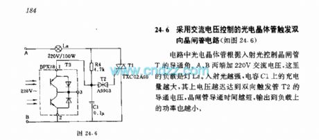
In this circuit, photoelectric transistor controls thyristor T's conduction angles by incident light. It adds 220V AC voltage on A,B, and La is the load. The stronger the incident light,the bigger thecharging on capacitorC1, the later voltage reaches Two-way trigger tube T2's conduction voltage, the shorter the thyristor's connection time, the lower the power of load.
(View)
View full Circuit Diagram | Comments | Reading(1142)
Two-way thyristor circuit integrated flip-flop TCA780
Published:2011/8/28 22:26:00 Author:Jessie | Keyword: Two-way thyristor, integrated flip-flop
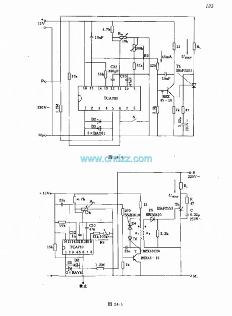
In this circuit, the control part and grid are segregated. The output pulse output by pin 15 of TCA780is amplified by trigger amplifier and added to pulse transformer primary winding. Secondary windings can supply 550μs triggering pulse, and the trigger current is 1A, andtrigger voltage is 2V.
(View)
View full Circuit Diagram | Comments | Reading(2679)
The static switch with integrated trigger TDAl024
Published:2011/8/28 22:24:00 Author:Jessie | Keyword: static switch , integrated trigger
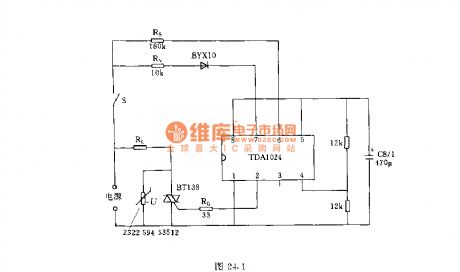
Thecircuitof integrated flip-flop TDA1024 will be connected afterswitch S closed. Whenever thepower gridvoltage is zero, it willproducea triggering pulse, and make the thyristor conduction, load current flow through the RL. When switch S is off, there is no current in load. In order to protect the Triac, it should be connected a varistor at both ends in parallel. The maximum power output of the circuit is 1400W, for example, if it uses thyristor BT139, the output power is up to 2000W; if it uses BTW41, the output power can be up to 5000W. (View)
View full Circuit Diagram | Comments | Reading(2968)
Switching rectifier basic structure block diagram
Published:2011/4/11 2:07:00 Author:may | Keyword: Switching rectifier, basic structure

Switching rectifier mainly consists of four parts: input circuit, power inverter, rectifying and wave-filtering circuit and control circuit, as shown in the diagram. Input circuit makes AC input voltage rectifying and wave-filtering more flat high voltage DC voltage. Then the AC input voltagepass power inverter and change it to high frequency pulse voltage, thenpass rectifying and wave-filtering circuit change the high frequency pulse voltage to steady DC voltage, then output to load. The function of control circuit is to guarantee the stabilisation and adjustable of output DC voltage. (View)
View full Circuit Diagram | Comments | Reading(1541)
Single end normal shock converter circuit principle diagram
Published:2011/4/11 2:12:00 Author:may | Keyword: Single end, normal shock, converter
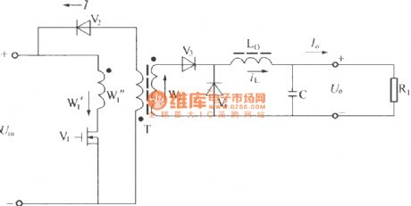
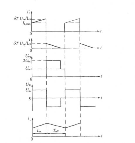
As shown in the diagram, when switch tube V1 is turn-on, input voltage Uin totally adds to justified of converter primary coil W1', induction voltage generates in degaussing iron ring W1'' make diode V2 cut-off, and induction voltage in secondary coil W2 make V3 turn-on, and sent the power of input current to inductance L0 and capacitance C and load; meanwhile it build up magnetizing current in converter, when V1 cut-off, V3 cut-ff, voltage direction on L0 is rollback andpass diode V4 to power supply to load continued, the magnetizing current in transformer willpass W1'', V 2 to release to input power source Uin and demagnetization; W1 has the function of clamp, the voltage on it is equivalent to input voltage Uin, before V1 turn- on again, demagnetizing current on T must release to zero, namely magnetic flux in T must reset, otherwise, transformer T will saturation and lead to the damage of V1. Normally, W1'=W1'', duty ratio of using two wires parallel winding coupled modes is <0.5, otherwise T will saturation. The wave form of single end normal shock converter is shown in the following diagram.
(View)
View full Circuit Diagram | Comments | Reading(1115)
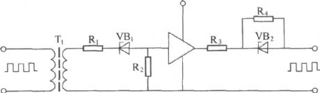
Forward converter consists of two RC circuit
Published:2011/11/10 2:05:00 Author:May | Keyword: Forward converter , two RC circuits

View full Circuit Diagram | Comments | Reading(1006)
The structure diagram of LDl001
Published:2011/11/10 2:06:00 Author:May | Keyword: structure
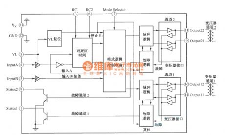
Because the frequency and duty factor changing of PWM signal is much larger, it can not convey simply through transformer.So SCALEis equipped with LDI001 logic drive interface. (View)
View full Circuit Diagram | Comments | Reading(1247)
The power supply circuit diagram of ENVISION EC-1468 SVGA multiple frequency color display
Published:2011/11/10 2:07:00 Author:May | Keyword: power supply, ENVISION, SVGA, multiple frequency, color display
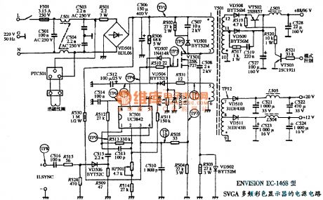
View full Circuit Diagram | Comments | Reading(1571)
| Pages:377/2234 At 20361362363364365366367368369370371372373374375376377378379380Under 20 |
Circuit Categories
power supply circuit
Amplifier Circuit
Basic Circuit
LED and Light Circuit
Sensor Circuit
Signal Processing
Electrical Equipment Circuit
Control Circuit
Remote Control Circuit
A/D-D/A Converter Circuit
Audio Circuit
Measuring and Test Circuit
Communication Circuit
Computer-Related Circuit
555 Circuit
Automotive Circuit
Repairing Circuit