
Circuit Diagram
Index 757
75_A_12_TO_16_VDC_REGULATED_POWER_SUPPLY
Published:2009/7/16 23:46:00 Author:Jessie
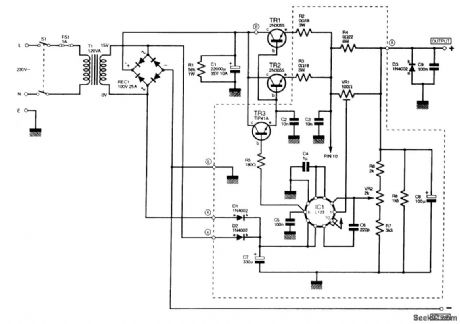
This supply uses an L123 regulator IC and a pair of 2N3055 power transistors as series-pass regulators VR1 is the current limit, and VR2 is the voltage control, The 2N3055 transistors and theTIP41A should be heatsinked because up to 50 W of dissipation can Occur. (View)
View full Circuit Diagram | Comments | Reading(2544)
±5_±15_AND__30_V_
Published:2009/7/16 23:45:00 Author:Jessie
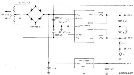
Provides all voltages needed for digitally controlled power supply that has voltage range from 0 to 25.5 V in 0.1-V increments. Highest positive voltage of +30 V is well above maximum output voltage that can be programmed.-D. Aldridge and N. Wellenstein, Designing Digitally-Controlled Power Supplies, Motorola, Phoenix, AZ, 1975, AN-703, p 4. (View)
View full Circuit Diagram | Comments | Reading(708)
SIMPLE_ADJUSTABLE_DC_SUPPLY
Published:2009/7/16 23:42:00 Author:Jessie
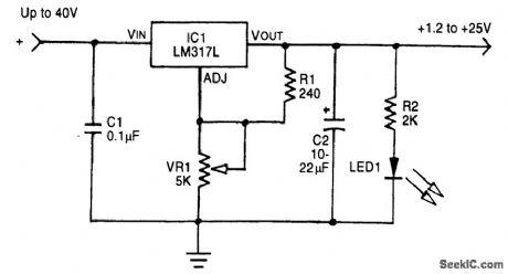
Using an LM317L IC, this regulator will find broad application where a simple adjustable supply is needed. The IC is a surface-mount type, but a different package style can be used. (View)
View full Circuit Diagram | Comments | Reading(1572)
DC_POWER_SUPPLY
Published:2009/7/16 23:42:00 Author:Jessie
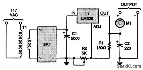
Here's the schematic for The Crusher dc power supply. The outputs are front-panel-mounted banana jacks. T1 is a 24- to 26-V transformer with 1- to 5-A capacity. C1 should be a minimum of 1000 μF per ampere of dc. C2 should be at least 100 μF (or larger). C2 helps maintain good transient response for transients that are too fast for the regulator, and 220 to 470 μF is recommended. BR1 is a 50-V bridge rectifier. U1 must be heatsinked. M1 is an ammeter of 0-5 A or 0-10 A full scale. The output voltage can be adjusted from about 1.2 to 30V via R2. Vout 1.26 (R2 /R1 + 1) volts. (View)
View full Circuit Diagram | Comments | Reading(2076)
5_AND_14_V_AT_1_A
Published:2009/7/16 23:42:00 Author:Jessie
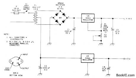
Regulated dual-voltage power supply serves for experimenting with TTL, CMOS, and linear IC projects. Higher-voltage regulator must be insulated from heat-sink.-A. Lorona, Dual Voltage Power Supply. 73 Magazine, Holiday issue 1976, p 146-147. (View)
View full Circuit Diagram | Comments | Reading(1487)
12_V_AT_5_A
Published:2009/7/16 23:40:00 Author:Jessie
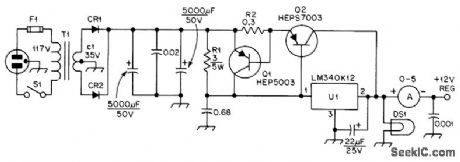
Uses National LM340K-12 mounted on external heatsink, with series-pass transistor Q2 boosting current rating to 5 A. Provides complete protection from load shorts; output drops suddenly to nearly zero when current exceeds 5 A. R2 is several feet of No, 22 enamel wound on phenolic form to make 0.3-ohm 60-W resistor. CR1 and CR2 are HEP R0103 or equivalent. Transformer is rated 18 V at 8 A.-C. R. Watts, A Crowbar-Proof 12-V Power Supply, QST, Aug. 1977, p 36-37. (View)
View full Circuit Diagram | Comments | Reading(899)
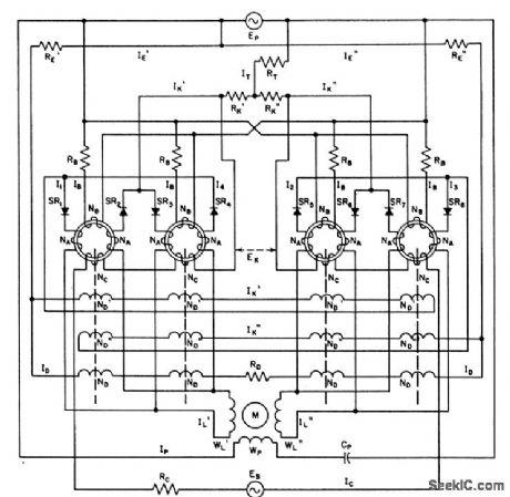
MAGNETICALLY_REGULATED_D_C_SUPPLY
Published:2009/7/17 1:24:00 Author:Jessie
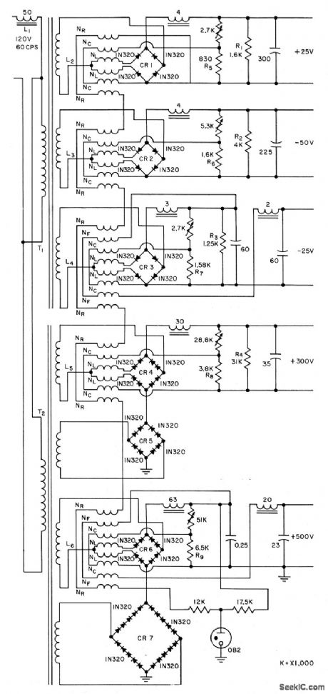
Magamps and saturating transformer maintain output regulation,within 3% for variation up to 20 V in supply voltage.Sillcon rectifiers in bridges convert a-c supply to d-c output at five different levels. Article gives all transformer winding data.-M. B. Meunier,Magnetic Amplifiers Regulate D-C Supply, Electronics, 31:9, p 68-70. (View)
View full Circuit Diagram | Comments | Reading(778)
1_MILLISEC_TO_30_HOURS
Published:2009/7/17 1:38:00 Author:Jessie
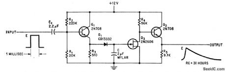
Input and out-put emitter-followers isolate fat, Extremely low lockage current through D1 and fet Q3 give circuit 30-hour time constant.-M. E. McGee, FET Circuit Stretches 1-MSEC Pulse to 30 Hours, Electronics, 38:7, p 87-88. (View)
View full Circuit Diagram | Comments | Reading(688)
PC_SIGNAL_GENERATOR
Published:2009/7/12 22:20:00 Author:May
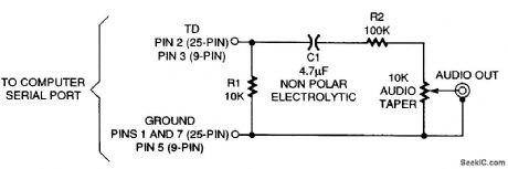
This circuit will produce audio from your PC. The trick is U-the ASCⅡ character U, that is.The hexadecimal value of U is 55, which in binary is 01010101 (with 8 data bits and no parity, or 7 data bits and even parity). The RS232 protocol specifies that the bits of an ASCII character are tran-mitted from least to most significant, preceded by a start bit (always 0) and followed by a stop bit (always 1). So, after adding the requisite start and stop bits, the result is 1010101010. Now, suppose a string of us is generated at the serial port at some steady rate. The result is a continuous series of alternating is and 0s-a square wave. The frequency of the signal will be half the baud rate, which by definition is the number of transitions per second. Each cycle of a square wave comprises two transitions, so, for example, a 9600-bps baud rate produces a 4800-Hz square wave. In practical terms, just about any computer should be able to deliver frequencies of 55, 150, 300, 600, 1200, 2400, and 4800 Hz, corresponding to the standard baud rates from 110 to 9600. The output of a serial port is nominally 24 V p-p, which is much too high a voltage to feed to the input of an audio amplifier. The circuit attenuates the signal to a more useful level, a variable 2-V p-p. The circuit also protects the computer from static electricity and voltage surges. Capacitor C1, a nonpolar unit, blocks dc because the serial port, when idling, outputs approximately -12 V.
(View)
View full Circuit Diagram | Comments | Reading(750)
LOGIC_PROBE_CIRCUIT
Published:2009/7/17 1:35:00 Author:Jessie
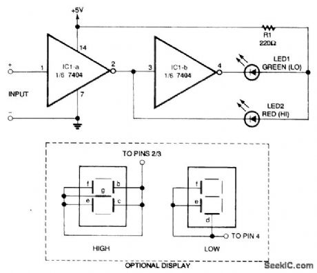
In this logic probe circuit, the red LED indicates logic high and the green indicates logic low, The optional use of an LED seven-segment readout is also shown. (View)
View full Circuit Diagram | Comments | Reading(1944)
FREEZER_SENTRY
Published:2009/7/12 22:19:00 Author:May
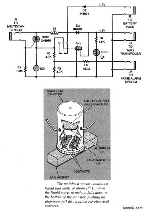
The heart of the circuit is SCR1, a silicon-controlled rectifier. Trigger voltage is supplied through J1 by the meltdown sensor when its contacts close. Resistor R1 is included to prevent any false triggering of SCR1 as a result of voltage fluctuations or noise from the power supply. Once SCR1 is triggered, it latches on, sounding the alarm buzzer until the reset switch (S1) is pressed. The reset switch interrupts current flow through the SCR, letting it turn off. Power for the circuit is supplied by a 12-Vdc wallmounted transformer, which is connected to J3. As long as the wall-mounted power supply is working, relay RY1 will be activated, opening its normally closed contact. Normal power will also be indicated by LED1, withR4 limiting the current flowthrough the light-emitting diode. If the ac powerfails, LED1 will go out and RY1 will deenergize, closing the relay's normally closed contacts. The relay contacts bypass SCR1, sounding the alarm. Backup power for that situation is supplied by a 12-V battery pack, which is connected to the circuit through J2 and D1. Diode D1 prevents the ac-derived power supply from attempting to charge the batteries, and D2 prevents the batteries from lighting the LED or energizing RY1 in the event of ac power failure. An additional feature of the circuit is that since the relay bypasses SCR1 during a loss of ac power, the reset button will not silence the alarm. Regardless of which type of failure caused the alarm to sound, R2 and R3 form a voltage divider that provides a 5-V signal to J4. (View)
View full Circuit Diagram | Comments | Reading(969)
CONVEYOR_BELT_OVERLOAD_PROTECTION
Published:2009/7/17 1:29:00 Author:Jessie
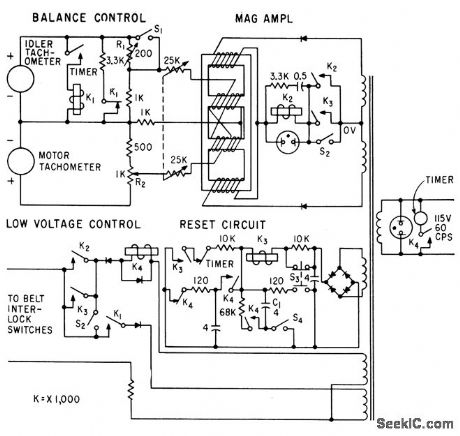
Tachometers monitor belt slip and feed four-leg magnetic amplifier which controls conveyor drive relay K2. If tachometer outputs do not match because of belt slip or belt failure, bridge becomes unbalanced, magamp output decreases, and K2 drops out.-F. R. Hulscher, Fail-Safe Circuits for Conveyor Sys tems, Electronics, 32:28, p 60. (View)
View full Circuit Diagram | Comments | Reading(1389)
TIME_TO_VOLTAGE_CONVERTER
Published:2009/7/12 22:18:00 Author:May
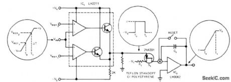
Dual comparator, solid-state switch, and fast FET opamp provide flexibility, range, and accuracy required for using converter in computer-controlled test system. IC2 operates as integrator and sample-and-hold circuit. Reference voltages of IC1, VREF1, and VFEF2 allow time measurements of signal having ehher positive or negative voltage levels or both. Floating output stdges of comparators provide voltage translation for FET switch S1. With S1 closed, IC2 integrates for time period during which input signal is below reference voltages. With S1 open, IC2 holds final voltage value. Measurement range is from 1 μs to several hours.-C. Wojslaw, Wide Range Time Measurements Simplified, EDN Magazine,-Feb.5, 1974, p 95-96.
(View)
View full Circuit Diagram | Comments | Reading(1189)
INFRARED_LOGIC_PROBE
Published:2009/7/17 1:29:00 Author:Jessie
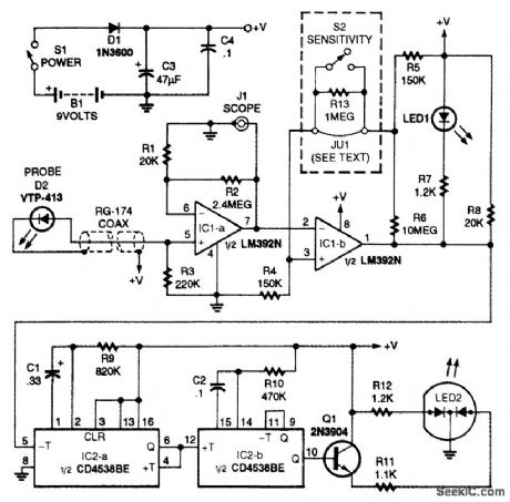
Infrared light detected by photodiode D2 is amplified by IC1-a. The value of R2 can be changed to decrease the sensitivity of the circuit, if your application demands it. Connector J1 provides an output to an oscilloscope for the display of the amplified photodiode signal. This is handy when checking the pulsed emitters in most remote controls. Voltage comparator IC1-b squares up signals from IC1-a to digital logic levels for IC2-a. LED1 and current-limiting resistor R7 indicate the presence of steady-state infrared and also function with pulsed emitters if the duty cycle is appropriate Monostable multivibrator IC2 conditions pulse trains with any period shorter than the time constant of R9 and C1 into a low-frequency waveform with a very high duty cycle. This provides pulses for LED2 that are constant in frequency and duty cycle, regardless of the high input frequency to IC2-a.Any frequency input to IC2-a with a period longer than the time constant of R9 and C1 creates IC2-b output pulses with the same width as before at the input frequency. Tricolor LED2 (a dual red/green device) functions as a pilot lamp and indicator for pulsed infrared sources. LED2 will always glow red and pulse amber (red + green) when infrared pulses are detected. The power source for the circuit is a 9-V battery. Alkaline batteries will provide many hours of operation because the circuit has low-power integrated circuits in place of S2 for most emitters. For certain devices, such as slotted optical switches, CD laser diodes, and reflective sensors, more sensitivity might be desirable. If you plan to use the probe for LEDs that operate below 0.5 mW, install S2 and R13-if not, you can in-stall a wire jumper on the board instead of the switch. (View)
View full Circuit Diagram | Comments | Reading(1003)
GENERIC_TAIAC_SWITCH_INTERFACE_FOR_RESISTIVEL_LOAD
Published:2009/7/17 1:29:00 Author:Jessie
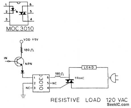
A TTL level input turns on the MOC3010 optocoupler and triggers the triac,applytng 120 Vac tothe load. (View)
View full Circuit Diagram | Comments | Reading(3392)
COMPUTER_CONTROLLED_A_D_CONVERTER
Published:2009/7/12 22:18:00 Author:May
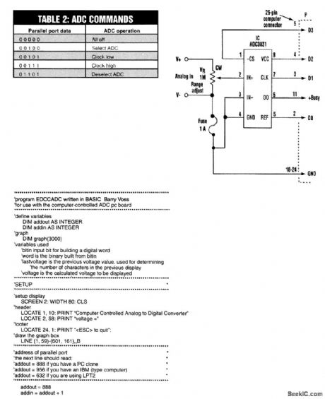

This simple, inexpensive computer-controlled A/D converter (ADC) plugs into a PC parallel port. The 8-bit peripheral device requires only seven components controlled to imponents and is imkplement and is completely controllde by a short BASIC program. (View)
View full Circuit Diagram | Comments | Reading(1148)
400_CPS_SERVO_MOTOR_DRIVE
Published:2009/7/17 1:28:00 Author:Jessie
Self-balancing single-stage magnetic amplifier has high response speed, excellent stability, excellent linearity, and freedom from drift. Provides half-cycle response as operational amplifier. Article gives winding data for saturable reactors.-J. Markus, Handbook of Electronic Control Circuits, McGraw. Hill, N.Y,, 1959, p 107. (View)
View full Circuit Diagram | Comments | Reading(793)
CUT_PHONE_LINE_ALARM
Published:2009/7/12 22:16:00 Author:May
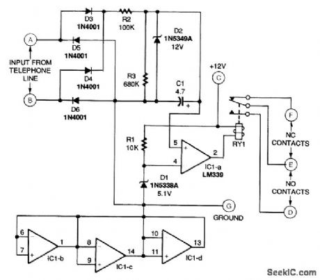
The figure shows the schematic diagram of the phone line monitor. Note that 12-Vdc power is connected to the unit via solder pads C (positive) and G(ground) on the PC board. This power should be supplied from your home security system, since it will have battery backup, and this will be as reliable as your base security system. The input from the telephone line is fed to pads A and B. Polarity is not important to the monitor because the input is rectified by the full-wave bridge rectifer formed by diodes D3 to D6. Connecting the phone line to the phone line monitor in no way diminishes phone senrtce', and its presence on the line will be unnoticed by you and those who call you. The rectified or polarized voltage from the bridge rectifier is fed to a long-time-constant filter formed by R2 and C1. This filter includes a zener diode (D2) that limits the voltage maximum charge on C1 to 12 V during normal operation. Resistor R3 provides a high-resistance shorting path to drain the charge from C1 when there is no input voltage. This resistor sets the time delay for activating the alarm. The trigger voltage for comparator IC1-a is generated by R1 and D1. Diode Dl is a 5.1-V zener whose output is fed to the inverting input (pin 4) of IC1-a. With the inverting input at 5.1 V, any voltage above 5.1 Y on the noninverting input (pin 5) will cause the output of the comparator to go high. Since the output of IC1 is tied to the relay coil of RY1 and the other end of the relay is tied to +12 Vdc, the relay coil is not energized. When the voltage from the input filter drops below 5.1 V, the out-put of IC1-a goes low and energizes the relay. The contacts of RY1 (either the normally open set or the normally closed set) could also be used to trigger the home's security system.
(View)
View full Circuit Diagram | Comments | Reading(1341)
CMOS_INTERFACE
Published:2009/7/17 1:27:00 Author:Jessie

This CMOS interface makes it possible for a simple or complex analog circuit to input data into a digital system. (View)
View full Circuit Diagram | Comments | Reading(786)
MAGAMPS_CONTROL_SCR_BRIDGE
Published:2009/7/17 1:27:00 Author:Jessie
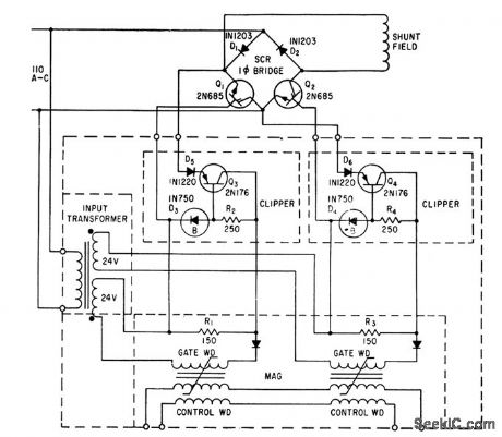
Single-phase bridge is controlled by two half-wave magnetic amplifiers each having a transistor emitter-follower used as clipper for each half-wave voltage output. Used for adjustable d-c field supply.-T. E. DeViney, Semiconductors Improve Reliability of Steel-Mill Control Equipment, Electronics, 34:23, p104-107. (View)
View full Circuit Diagram | Comments | Reading(922)
| Pages:757/2234 At 20741742743744745746747748749750751752753754755756757758759760Under 20 |
Circuit Categories
power supply circuit
Amplifier Circuit
Basic Circuit
LED and Light Circuit
Sensor Circuit
Signal Processing
Electrical Equipment Circuit
Control Circuit
Remote Control Circuit
A/D-D/A Converter Circuit
Audio Circuit
Measuring and Test Circuit
Communication Circuit
Computer-Related Circuit
555 Circuit
Automotive Circuit
Repairing Circuit