
Circuit Diagram
Index 755
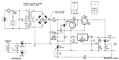
50_300_V_VARIABLE_AT_100mA
Published:2009/7/16 22:51:00 Author:Jessie

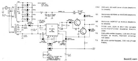
Solid-state version of regulated high-voltage supply for tube circuit has ad adjustable current-limiting, instant turn-on, and long component life. Small variable autotransformer in primary circuit of high-voltage transformer is mechanically ganged to DC voltage-control pot connected to pin 8 of U1 to keep input-to-output voltage difference nearly constant. Differential voltage across Q1 never exceeds 100 V so power dissipation of Q1 is only 5W maximum. Regulator circuit is designed around Motorola MC1466L or MC1566L floating regulator powered by 25-V supply having no common connection to ground. Use 600-V rating for 0.33 μF from T3 to ground.-H. Olson, Regulated, Variable Solid-State High-Voltage Power Supply, Ham Radio, Jan. 1975, p 40-44. (View)
View full Circuit Diagram | Comments | Reading(3566)
CONSTANT_DUTY_CYCLE
Published:2009/7/16 22:51:00 Author:Jessie
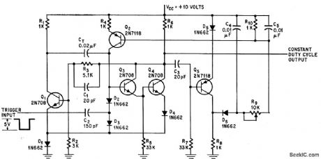
Width of output pulse varies with frequency to keep duty cycle constant at preadjusted value from 25% to 75%, over input trigger range of 100 to 5,000 pps. Q1, Q3, and Q4 form one mvbr, and Q5 is second mvbr. Q2 is voltage-to-current converter.-G. P. Klein, Duty Cycle is Constant at any Trigger Frequency, Electronics, 38:15, p 62-63. (View)
View full Circuit Diagram | Comments | Reading(814)
001_MICROWATT_40_CPS_MVBR
Published:2009/7/16 22:51:00 Author:Jessie
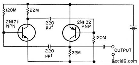
Both npn and pnp transistors conduct at same time for part of cycle, and both are cut off for remainder of cycle, so average power consumed is much less than when one transistor always conducts. Frequency is 40 cps. With 0.6-V supply furnishing 0.015 microamp, total power consumption is 0.009 microwatt. -W. G. Shepard, A 0.01 Microwatt Multivibrator, EEE, 10:8, p 29. (View)
View full Circuit Diagram | Comments | Reading(761)
MAGNETRON_BEAM_SWITCHING
Published:2009/7/16 22:49:00 Author:Jessie
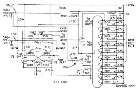
First trigger pulse switches beam to first position, and each succeeding trigger advances beam one position, until reset pulse zeroes V11 for repetition of switching sequence. Succeeding switching-circuit output pulses are thus time-coincident with succeeding amplitude portions of input signal, for pulse amplitude measurement.-J. F. Lyons, Jr., Analyzing Multipath Delay in Communications Studies, Electronics, 32:36, p 52-55. (View)
View full Circuit Diagram | Comments | Reading(728)
SYNCHRONIZED_ASTABLE_MAIN_GATE_MVBR_
Published:2009/7/16 22:49:00 Author:Jessie
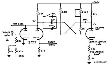
Used in combination search and gun-laying radar. Different gate lengths are obtained by switching capacitors. Provides positive unblanking gate.-NBS, Handbook Preferred Circuits Navy Aeronautical Electronic,Equipment, Vol. 1, Electron Tube Circuits, 1963, p N10-4. (View)
View full Circuit Diagram | Comments | Reading(655)
BASIC_HALF_BRIDGE_CONVERTER_CIRCUIT
Published:2009/7/16 22:48:00 Author:Jessie
A popular and established switching power-supply topology is the half-bridge converter, The same converter will work from either a 120- or 240- Vac input; it is simply necessary to change terminals. It is cost-effective over the 150- to 500- W range, and offers very good output noise characteristics and excellent transient response. (View)
View full Circuit Diagram | Comments | Reading(1022)
DOUBLE_COUPLED_MAIN_GATE_MVBR_1
Published:2009/7/16 22:48:00 Author:Jessie
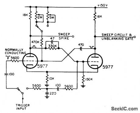
Uses both cathode and plate-to-grid coupling, with gate length changed by switching of potentiometers. Differentiated negative gate from delay mvbr is applied as trigger to grid of normally conducting tube if undelayed range sweep is desired, or to grid of normally-off tube when delayed sweep is used.-NBS, Handbook Preferred Circuits Navy Aeronautical Electronic Equipment, Vol.1, Electron Tube Circuits, 1963, p N10-3. (View)
View full Circuit Diagram | Comments | Reading(686)
5_V_SUPPLY
Published:2009/7/16 22:48:00 Author:Jessie
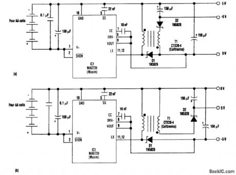
The inverter circuit substitutes a transformer with two matched windings for the usual inductor (see figure a), When IC1's internal switch turns off, the circuit impresses Vout plus a diode drop across each winding. With the reference connection properly chosen, as shown, the second (right-hand) winding can generate an additional supply voltage (-5 V, in this case). Vout (pin 8) is the feed-back connection. For stability, the regulated output (5 V, in this case) should have the heavier load. It usually does because the negative rail in most systems is only a bias supply. But if the system demands more load current from the -5-V output, the second winding should be reconnected to produce the 5-V output (see figure b). The transformer should have side-by-side bifilar windings for best coupling. The V- value (nominally -5 V) depends on load currents and the transformer turns ratio (which can deviate from 1:1). Loads of 5 to 50 mA at 5 V, for example cause a V- change of less than 300 mV-less than that expected from a charge pump. When unloaded, V- increases because of rectification of the ringing that occurs when D2 turns on. (View)
View full Circuit Diagram | Comments | Reading(849)
SOLAR_POWERED_INSECT_CONTROLLER
Published:2009/7/16 22:48:00 Author:Jessie
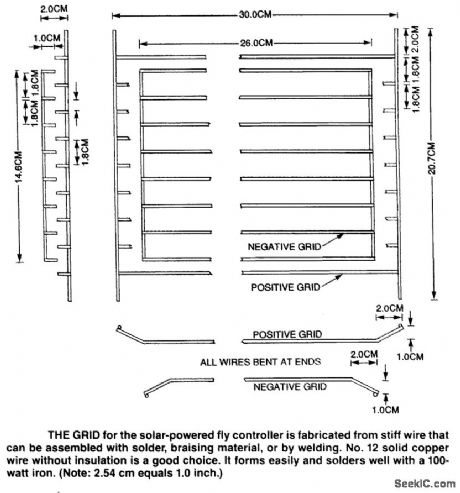
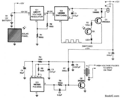
The circuit for the solar-powered controller consists of a switching circuit, a pulsing circuit, and a high-voltage output circuit. The external power components are a 1- to 5-W solar panel and a 12-V motorcycle or camcorder battery. The output of the high-voltage ignition coil connects to a net-work of paralleled electrodes, called a grid, upon which flies land and are destroyed. Voltage input to the LM3909 LED-flasher/oscillat or (IC2) is kept at 6 to 9V by a LM317T voltage regulator (IC1).The exact voltage is not crucial as long as it is regulated. The LM3909 produces a series of pulses that are coupled to a 2N2222A transistor (Q1) to form a switching circuit. An output of positive pulses from IC2 to the 2N2222A transistor boosts the pulse current so that it closes a 5-V relay (RY1) for approximately 0.1 s at intervals of 1 to 2 s. Diode D1 shunts out high-voltage spikes
produced by the switching voltage across the relay's coil. The switching circuit is turned off at night or during periods of heavy cloud cover by phototransistor Q3, whose internal resistance increases as the ambient light diminishes. This reduces the positive bias on Q1's base, causing the transistor to cut off. LED1 serves as a voltage-dropping device. Single-pole, single-throw relay RY1 provides brief pulses of the 12-V battery voltage to IC3, an NE755 timer that is wired as a free-running audio-frequency pulse generator. The pulses are amplified by a 2N3055 power amplifier transistor, Q2.The output of Q2 drives an automobile ignition coil, T1, to generate the high-voltage pulses for the external grid. The output voltage at the secondary winding of T1 is approximately 12,000Vp-p. The circuit is powered by a 12-V rechargeable lead-acid or nickel-cadmium battery. A 1-W or better solar panel of the type used to keep automobile batteries charged should be used to eliminate the need to recharge the battery frequently. (View)
View full Circuit Diagram | Comments | Reading(2310)
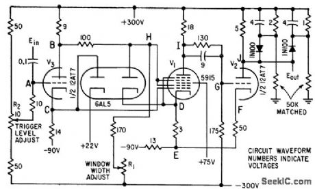
TUNNEL_DIODE_PULSEHEIGHT_DISCRIMINA_TOR
Published:2009/7/16 22:47:00 Author:Jessie
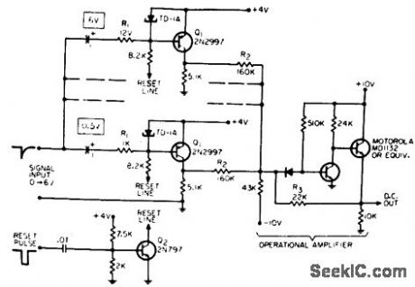
Used to analyze 30,nsec pulses varying in height from 0 to 6 v peak, over temperature range of -20 to +60°C, Ten stages were connected in parallel and 0.5.v steps used for 0 to 5 v output range. When tunnel diode is triggered at its predetermined level, Q1 delivers fixed current to operational amplifier. As input pulse height increases, more and more tunnel diodes are triggered, and current to operational amplifier increases linearly.-J. D. Nickell, tunnel-Diode Pulse-Height Discriminator, EEE, 13:9, p 75. (View)
View full Circuit Diagram | Comments | Reading(967)
SHOCK_SPECTRUM_ANALYZER
Published:2009/7/16 22:45:00 Author:Jessie
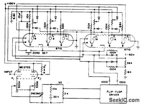
Inexpensive peak memory unit has indefinitely long memory, to retain information long enough for dl channels to be recorded. Shock spec trum of input pulse is then defined by peak voltages across capacitors in all memory units. Output is d-c level for automatic recording or plotting.-D. F. Palmer, Shock Spectrum Analyzer, PEE, 11:3, p 118-119. (View)
View full Circuit Diagram | Comments | Reading(766)
137_V_AT_5_A
Published:2009/7/16 22:45:00 Author:Jessie
Output is constant within 0.7 V for AC line range of 98 to 128 VAC, and regulation is within tenths of a volt from 0 to 5 A. Design includes short-circuit, over current, and overvoltage protection. Uses series-pass transistor to increase current-carrying capability of regulator. Transistors are mounted on but insulated from heatsink, C2 is essential to prevent oscillation under certain conditions. Use gallium arsenide phosphide LED. Article tells how to determine exact trip point of SCR crowbar. -B. Meyer, Low-Cost All-Mode-Protected Power Supply, Ham Radio, Oct. 1977, p 74-77.
(View)
View full Circuit Diagram | Comments | Reading(1125)
SCHMIDT_TRIGGER_MEMORY_CELL_CIRCUIT_1
Published:2009/7/16 22:45:00 Author:Jessie
View full Circuit Diagram | Comments | Reading(569)
AMPLITUDE_WINDOW
Published:2009/7/16 22:44:00 Author:Jessie
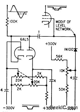
Provides trigger on negative portive of input signal or noise, for slicing portion out of input signal for use with amplitude analyzer in determining probability amplitude density functions.-T. A. Bickart, Amplitude Slicer for Signal Analysis, Electronics, 32:9, p 64-65. (View)
View full Circuit Diagram | Comments | Reading(774)
BASIC_PUSH_PULL_CONVERTER_CIRCUIT
Published:2009/7/16 22:44:00 Author:Jessie
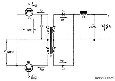
The push-pull converter consists of two forward converters working 180° out of phase. Both halves of the push-pull Converter deliver current to the load at each half cycle, and the inductor stores energy. Diodes D1 and D2 conduct simultaneously between transistor conduction, effectively short-circuiting the secondary isolation transformers. Acting as flywheel diodes, these diodes deliver useful power to the output. (View)
View full Circuit Diagram | Comments | Reading(1844)
SIGNAL_AMPLITUDE_ANALYZER
Published:2009/7/16 22:43:00 Author:Jessie
Width of rectangular output pulse is proportional to time spent by signal between specified voltage levels. Used to determine probability amplitude density functions,-T. A. Bickart, Amplitude Slicer for Signal Analysis Electronics 32:9, p 64-65. (View)
View full Circuit Diagram | Comments | Reading(789)
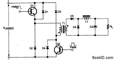
FEEDBACK_CONTROL_FOR_MAX253
Published:2009/7/16 22:42:00 Author:Jessie
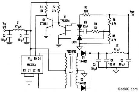
The MAX253 and associated 76253 transformers were designed to allow easy implementation of simple dc-to-dc converter circuits. The main problem with the basic circuit is that there is no feed-back, resulting in no control over the output voltage at light loads. When transformer isolators designed for 1-W power levels are used, output voltages can be observed rising above 5.5 V at less than 20-percent load. The circuit provides feedback control from the output via an optoisolator and voltage-reference device in a single pack (TPS5094). This results in an output voltage that is static at light loads. The circuit uses the internal TL431 reference devices of the TPS5904 to set a value at which the optoisolator is switched (Vref = 2.51 V). Using two 4.7-kΩ resistors (R5 and R6) gives an ideal output voltage of 5 V; with only 500μA of drain current, the measured value was 4.95 V. The output of the optoisolator then controls the shutdown pin (SD) on the MAX253, via the ZTX451 buffer transistor, and switches the device off when the output voltage exceeds the predefined value. Therefore, the circuit works in a burst mode at light loads, with the switching being turned on and off as necessary. As the load increases, the device eventually reaches the stage where switching is occurring all the time. (View)
View full Circuit Diagram | Comments | Reading(906)
±14_V_TRANSFORM_ERLESS
Published:2009/7/16 22:41:00 Author:Jessie
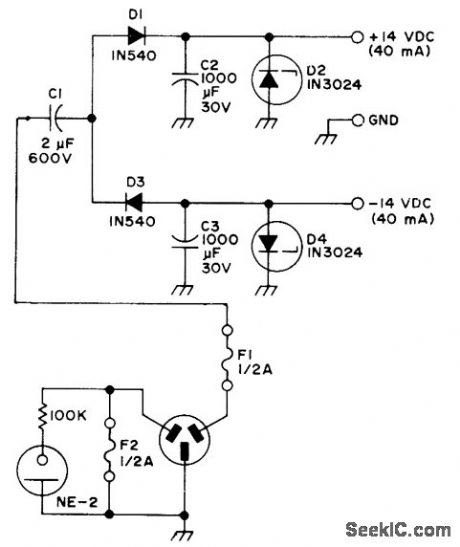
Simple low-current regulated supply requires no power transformer. Output current can be increased by using better filtering. Second ground prong is connected through fuse to grounded center conductor of AC line to guard against faulty AC wiring. If wiring is reversed, fuse will disable power supply and neon fault indicator will come on.-D. Kochen, Transformerless Power Supplies, 73 Magazine, Sept. 1971, p 14-17. (View)
View full Circuit Diagram | Comments | Reading(683)
SIMPLE_INTERCOM
Published:2009/7/16 22:41:00 Author:Jessie
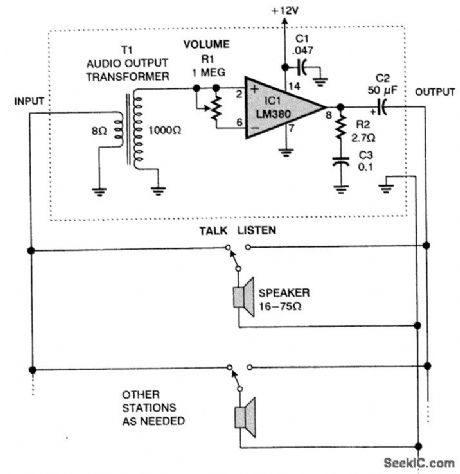
This intercom uses an LM380 IC to act as an amplifier and speaker driver (View)
View full Circuit Diagram | Comments | Reading(878)
Linear Pulse Width Modulator circuit (555)
Published:2011/8/4 8:47:00 Author:nelly | Keyword: Linear, Pulse Width, Modulator
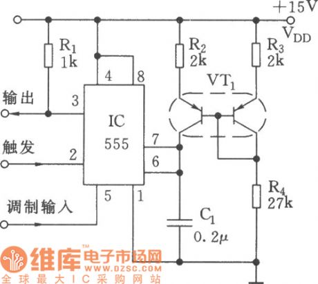
Linear Pulse Width Modulator circuit (555) (View)
View full Circuit Diagram | Comments | Reading(1690)
| Pages:755/2234 At 20741742743744745746747748749750751752753754755756757758759760Under 20 |
Circuit Categories
power supply circuit
Amplifier Circuit
Basic Circuit
LED and Light Circuit
Sensor Circuit
Signal Processing
Electrical Equipment Circuit
Control Circuit
Remote Control Circuit
A/D-D/A Converter Circuit
Audio Circuit
Measuring and Test Circuit
Communication Circuit
Computer-Related Circuit
555 Circuit
Automotive Circuit
Repairing Circuit