
Circuit Diagram
Index 791
SOLID_STATE_LATCHING_RELAY_CIRCUIT
Published:2009/7/17 4:07:00 Author:Jessie
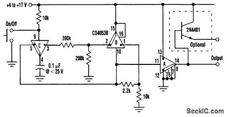
A multitude of simple circuits perform switch debouncing because there are many ways to implement a toggling latch. The circuit illustrated here merges these functions into one topology, is extremely tolerant of power-supply variation (it works fine over more than a 3:1 range of supply voltage), and, most importantly, is unusual. The IC used in this case is the 4053B triple CMOS SPDT switch. Section B acts as a bistable latch and stores the current ON/OFF state of the relay. The 2.2-kΩ resistor between pins 1 (the ON terminal of the switch) and 10 (the control input) provides positive feedback that sustains the switch in whichever state it finds itself. Thus, if the latch is ON, pin 1 will be switched to pin 15 and, thereby, the positive rail. This will reinforce the positive state of pin 10 and the ON state of the switch. If, on the other hand, the latch is OFF, then the connection of pin 1 to pin 15 will be broken and the 10-kΩ pull-down resistor will drag pin 1 to ground. This will pull pin 10 low, in turn, holding the latch in the OFF state. Meanwhile, pin 2 will output the logic inverse of the signal appearing in pin 1. This signal communicates to pin 3 and, if the control push button is open, will connect to pin 4 and charge the capacitor to a state opposite that of the latch. There matters will rest until someone presses the button. This will connect the capacitor to pin 10 and toggle the Latch state. 4053B section A serves as an output buffer and has an output impedance of about 200 Ω when run with a 5-V supply and 100 Ω when run with a 12-V supply. If this is insufficient for the application, a transistor emitter-follower, like that illustrated, will boost output capability to beyond 0.1 A. (View)
View full Circuit Diagram | Comments | Reading(2582)
TRANSISTOR_SENSOR_TEMPERATURE_MEASURER
Published:2009/7/11 0:34:00 Author:May
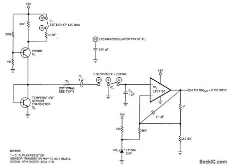
Using the fact that the I/BE of a transistor shifts 59.16 mV per decade of current at 25℃. This constant is 0.33%/'℃. This VBE-vs.-current relationship holds true regardless of the VBE absolute value. IC, an LT1043, acts as an oscillator and switches a current source (Q1) at a 10:1 ratio. The stepped 10:1 current drive is translated to temperature by IC2, Q2, and the associated components. Accuracy is 11%. No compensation is needed if Q2 is changed. (View)
View full Circuit Diagram | Comments | Reading(1579)
POLARITY_SENSITIVE_RELAY_CIRCUIT
Published:2009/7/17 4:07:00 Author:Jessie
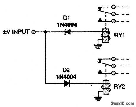
When a positive voltage is input to the circuit, relay RY1 is activated; when a negative voltage is input, RY2 is activated. (View)
View full Circuit Diagram | Comments | Reading(1639)
OVER_TEMPERATURE_SWITCH
Published:2009/7/11 0:32:00 Author:May

The output goes high when a preset tempera-ture is exceeded. A fixed half-supply reference voltage feeds a reference current to the inverting input, and a variable current is fed to the noninvert-ing input. Resistor R6 is a negative-temperature-coefficient (NTC) thermistor, so the potential at the junction of R5 and R6 rises with temperature. The op amp will switch high when that voltage exceeds the half-supply value. The trip temperature can be preset via R5. (View)
View full Circuit Diagram | Comments | Reading(1001)
Ionization_chamber_smoke_detector_using_McMOS_alarm_oscillators_
Published:2009/7/17 4:07:00 Author:Jessie
Ionization-chamber smoke detector using McMOS alarm oscillators (courtesy Motorola Semiconductor Products Inc.). (View)
View full Circuit Diagram | Comments | Reading(2831)
50_μA_SOLID_STATE_RELAY
Published:2009/7/17 4:06:00 Author:Jessie


The relay circuit described here reduces the control current to 50 μA, but can switch up to 600 W of 120-Vac power. The circuit uses a conventional 10-A, 400-V triac. The triac gate current is routed through a small bridge rectifier, a 15-V zener diode, a sensitive SCR (Q2), and a 180-Ω resistor (R2). The circuit allows a small SCR to control ac current through the triac's gate terminal. The voltage needed to control the SCR's gate terminal is developed by rectifying and filtering the ac voltage across the triac. Capacitors C2, C4, and C5, resistor R3, bridge rectifier BR2, and zener diode D2 form the rectifier circuit. C5 and D2 filter and limit the supply voltage to about 8 V, while the 470-Ω resistor R3 limits the charging current. To develop a slightly higher voltage (up to 30 V p-p), a 15-V zener diode (D1) is inserted in series with the SCR. D1 delays the triac's conduction trigger point each half cycle and produces only a slight reduction in rms power to the load. The dc control voltage, produced by the rectifier circuit, is switched to the SCR's gate using a sensitive Darlington-type optoisolator (A1)i Only about 50 μA of LED current in the isolator is needed to fully turn on the SCR. (View)
View full Circuit Diagram | Comments | Reading(1005)
WATER_LEVEL_MONITOR
Published:2009/7/17 4:06:00 Author:Jessie
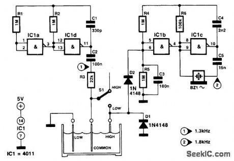
This circuit was devised to produce art audible alarm when a water tank was approaching empty. The circuit consists of two conventional CMOS oscillator gate pairs, as found in the textbooks. With the switch in the LOW position, gates IC1a and IC1d provide an alternating current flow through C2, R3, the common electrode, the water, and the low electrode, to earth. When the water level drops, the circuit to earth is interrupted, and the ac then fed via S1 to the junction of D1 and D2. This charges C3 so that pin 5 of IC1b goes positive, causing gates IC1b and IC1c to start oscillating. The audible transducer is an ac buzzer. The switch is then moved to the HIGH position. Pin 6 of IC1 is then at ground potential via R5, waiting for the tank to fill and connect the common and high electrodes via the water. The ac then flows through D2 to once again sound the alarm. The pump is turned off and S1 is restored to sense empty once more. The rate of charge of capacitor C3 can be changed by altering the value of R3. The power supply for the circuit can be from 5 to 12 V. (View)
View full Circuit Diagram | Comments | Reading(1171)
TEMPERATURE_SENSOR
Published:2009/7/11 0:31:00 Author:May

The AD537 uses its two reference outputs-one fixed at 1 V, the other of which varies with tempera-ture (1 mV per °K). At 0℃, the 1-V reference multiplied by 0.273 will balance this voltage and produce a zero output. The scale in this circuit is 10 Hz/℃. Output from, as well as power to, the circuit, is fed via a two-wire twisted pair. A frequency counter is used as a readout. (View)
View full Circuit Diagram | Comments | Reading(0)
UNDER_TEMPERATURE_SWITCH
Published:2009/7/11 0:30:00 Author:May
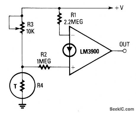
The reference current is fed from the supply voltage via R1, to the inverting terminal, and the variable (noninverting) current is supplied from the junction of R3 and R4. Because the value ofR1 is approximately double that of R2, and generates a current that is proportional to the supply voltage, the trip temperature (preset via R3) is independent of the supply voltage. (View)
View full Circuit Diagram | Comments | Reading(872)
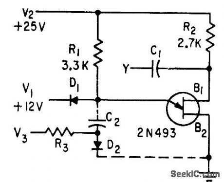
TRANSISTOR_UJT_MVBR
Published:2009/7/17 4:06:00 Author:Jessie
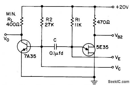
Uses low-cost 7A35 silicon mesa transistor.- Transistor Manual, Seventh Edition, General Electric Co, 1964, p 341. (View)
View full Circuit Diagram | Comments | Reading(624)
TGS_gas_smoke_detector_with_2_minute_time_delay_using_a_McMOS_latch_
Published:2009/7/17 4:05:00 Author:Jessie

TGS gas/smoke detector with 2-minute time delay using a McMOS latch (courtesy Motorola Semiconductor Products Inc.). (View)
View full Circuit Diagram | Comments | Reading(817)
UJT_BISTABLE_WITH_CLAMP
Published:2009/7/17 4:05:00 Author:Jessie
Clamping diode holds emitter voltage below peak-point voltage. When negative trigger at base B2 turns on transistor, D2 is back-biased and R1 becomes emitter load. Operation is stable if capacitance between emitter and base B1 is kept below critical value.-T. P. Sylvan, Bistable Circuits Using Unijunction Transistors, Electronics, 31:51, p 89-91. (View)
View full Circuit Diagram | Comments | Reading(918)
SIMPLE_TEMPERATURE_INDICATOR
Published:2009/7/11 0:29:00 Author:May

For the absolute measurement of temperatures, a thermometer is indispensable. However, in many situations, an absolute value is not needed and a relative indication is sufficient. It would be a further advantage if a green light would indicate that all is well as far as temperature is concerned. As the tempera-ture rises, the light should change color slowly to indicate that the equipment is getting too hot.This circuit does this and works directly from the mains. The indicator proper is a two-color LED (Dl), while the sensor is a combination of a negative-temperature coefficient (NTC) and a positive-tem-perature coefficient (PTC) resistor (R4 and R3, respectively).At a relatively low temperature, the value of R3 is low and that of R4 is high. During the positive half cycle of the mains voltage, a voltage will exist across R3/D2 that is sufficiently high to cause the green section of D1 to light. The value of R3 has been chosen to ensure that during the negative half cycle of the mains voltage, the potential across it is too low to cause the red section of D1 to light.If the temperature rises, the value of R4 diminishes and that of R3 rises. Slowly, but surely, the green section will light with lesser and lesser brightness. At the same time, the red section lights with greater and greater brightness until ultimately only the red section will light.Resistor R2 and capacitor C1 ensure that the current drawn by the LEDs does not become too large. This arrangement keeps the dissipation relatively low. Both R3 and R4 should be of reasonable dimen-sions-approximately 6 mm in diameter, not less. At 25℃, the NTC must be 22 to 25 kΩ and the PTC must be 25 to 33 0. The circuit should be treated with great care because it carries the full mains voltage. (View)
View full Circuit Diagram | Comments | Reading(1181)
MONO_WITH_NEGATIVE_RECOVERY_TIME
Published:2009/7/17 4:04:00 Author:Jessie
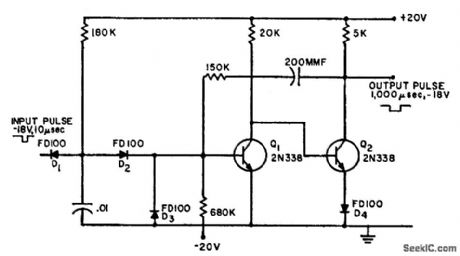
Will respond to input pulses occurring even before end of output pulse, which in effect gives negative recovery time. If circuit begins normal 1,000-microsec cycle and another trigger pulse arrives in 500 microsec, output pulse will last 1,500 microsec, or 500 microsec longer than usual. In other words, output pulse continues for 100 microsec after last trigger pulse. Input pulses should be of standardized voltage and long enough to discharge 0.01-mfd capacitor.-Monostable Circuit with Negative Recovery Time, Electronic Circuit Design Handbook, Mactier Pub. Corp., N.Y., 1965, p 72. (View)
View full Circuit Diagram | Comments | Reading(740)
THERMAL_MONITOR
Published:2009/7/11 0:27:00 Author:May

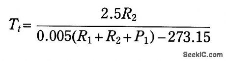
Unitrode's UC1730 family of integrated circuits is designed for use in a number of thermal monitoring applications. Each IC combines a temperature transducer, a precision reference, and a temperature com-parator to allow the device to respond with a logic output if temperatures exceed a predetermined level.The monitor presented here is based on a UC3730T and it is intended to be fitted to a heatsink. Although the supply to the device can be as high as 40 V, 5- to 8-V is chosen here, because it is normally readily available in the equipment where the monitor will be used (power amplifiers, power supplies, etc.).The threshold temperature, Tt, in ℃, is determined by:The temperature can be preset with Pl to values between -1℃ and + 100℃. The indicator is formed by a bicolor LED and controlled by transistors T1 and T2. Resistors R4 and R5 limit the current through the LED. When the temperature of the heatsink is below the threshold temperature, the ALD (alarm delay) output, pin 4, is logic low so that T1 is switched off and the green LED lights. (View)
View full Circuit Diagram | Comments | Reading(1236)
WATERING_CONTROL_WITH_RF_MOISTURE_SENSING
Published:2009/7/17 4:03:00 Author:Jessie


The moisture sensor does not depend on the ohmic resistance of the soil to activate the water valve. Instead, a VLF oscillator circuit with its tuned inductor buried In the soil senses the moisture content by absorption,Transistor Q2,L1,C3,and 04,make up a simple Hartley oscillator The circuit oscillates at about 16 kHz Transistor Q1,in an emitter-follower configuration,isolates the output circuit from loading or influencing the oscillator circuit Diodes D1 and D2 convert the RE Signal to dc to supply bias current for Q3,which operates the water-valve relay as long as the oscillator's output signal is sufficient to turn it on The oscillator,s sensitivity to varying soil conditions is set by R6,a 10-turn trimmer potentiometer The inductor,L1,consists of a 100-ft length of #26 plastic-covered wire wound in a 4-inch loop and kept together with electrical tape The loop is one area where much can be gained by experimenting,A pancake loop might be more sensitive or a different-shaped loop might work better,Also try different oscillator frequencies. (View)
View full Circuit Diagram | Comments | Reading(966)
TEMPERATURE_CONTROLLER
Published:2009/7/11 0:21:00 Author:May
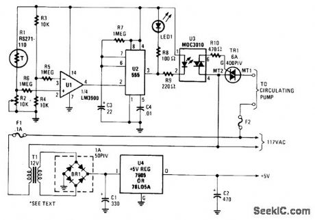
A thermistor (R1) is compared with a reference (R2) in a Wheatstone-bridge circuit. Comparator U1's output goes high, which triggers U2. U2 is a delay of about 25 s. After 15 s, LED1 lights, U3 actuates, triac TR1 triggers, and turns on a hot water pump. This system was used with a hot-water heater. (View)
View full Circuit Diagram | Comments | Reading(0)
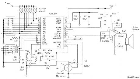
RECORD_PLAYBACK_CIRCUIT_WITH_AUTOMATIC_POWER_DOWN
Published:2009/7/17 4:03:00 Author:Jessie

Many applications for sound recording and reproduction, where battery power is necessary, require minimum power consumption. A circuit that achieves automatic power down in a record-and-play application is shown. The cross-coupled latch, consisting of a 4093 Schmitt trigger quad two-input NAND package (U2A and U2B), works to control the PD and CB pins for the Play mode. Circuitry for the Record mode consists of U2C and U2D plus several support components. To start the Record cycle, S2 supplies the ground to the microphone circuit and takes the input to U2D low. The Schmitt Trigger action of U2 debounces the logic input to the ISD1020A. (View)
View full Circuit Diagram | Comments | Reading(1122)
THERMOCOUPLE_TEMPERATURE_CONTROL
Published:2009/7/11 0:16:00 Author:May
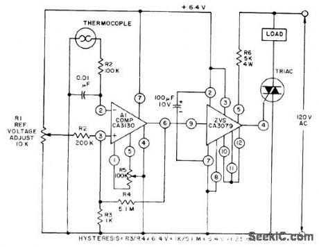
This control, with zero-voltage load switching, uses a CA3130 BiMOS op amp and a CA3079 zerovoltage switch. The CA3130, used as a comparator, is ideal because it can compare the low voltages generated by the thermocouple to the adjustable reference voltage over the range or0 to 20 mV. (View)
View full Circuit Diagram | Comments | Reading(0)
TGS_gas_smoke_detector_using_a_McMOS_gated_oscillator_for_triac_control
Published:2009/7/17 3:58:00 Author:Jessie

TGS gas/smoke detector using a McMOS gated oscillator for triac control (courtesy Motorola Semiconductor Products Inc.). (View)
View full Circuit Diagram | Comments | Reading(742)
| Pages:791/2234 At 20781782783784785786787788789790791792793794795796797798799800Under 20 |
Circuit Categories
power supply circuit
Amplifier Circuit
Basic Circuit
LED and Light Circuit
Sensor Circuit
Signal Processing
Electrical Equipment Circuit
Control Circuit
Remote Control Circuit
A/D-D/A Converter Circuit
Audio Circuit
Measuring and Test Circuit
Communication Circuit
Computer-Related Circuit
555 Circuit
Automotive Circuit
Repairing Circuit