
Circuit Diagram
Index 801
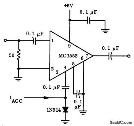
Video_amplifier_with_AGC_using_an_MC1553_wide_band_amplifier
Published:2009/7/17 4:42:00 Author:Jessie


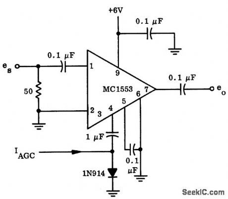
Video amplifier with AGC using an MC1553 wide-band amplifier (courtesy Motorola Semiconductor Products Inc.). (View)
View full Circuit Diagram | Comments | Reading(835)
CURSOR_FOR_TV_TYPEWRITER
Published:2009/7/10 22:04:00 Author:May
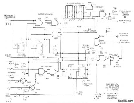
Complete CMOS logic cursorand update system is shownfor system using RAM memory,direct memory access, and writing during vertical intenral for displaying 512 characters per page on TV screen, Extemal 7.5-Hz source is required to make undedine cursorflash to indicate position at which next character will be entered on screen.-D, Lancaster, TV Typewriter Cookbook, Howard W .Sams,Indianapoils,IN,1976,p 128-129 (View)
View full Circuit Diagram | Comments | Reading(716)
Video_amplifier_with_AGC_using_an_MC1552_1553_wide_band_amplifier
Published:2009/7/17 4:41:00 Author:Jessie
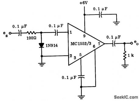
Video amplifier with AGC using an MC1552/1553 wide-band amplifier (courtesy Motorola Semiconductor Products Inc.). (View)
View full Circuit Diagram | Comments | Reading(712)
ELECTROSTATIC_DEFLECTIO_AMPLIFIER
Published:2009/7/10 22:03:00 Author:May
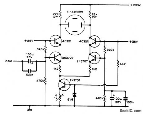
Combines frequency response of cascode am pilfer with linearity of long-tailed pair fed by constant current, Adjust R for 3 mA through each load resistor. Output transistors require small heatsinks.-G. A Johnston, Deflection Amplifier, Wireless World, Nov. 1973, p 560. (View)
View full Circuit Diagram | Comments | Reading(1420)
Norton_AND_gate_and_NAND_gate_with_high_fan_in
Published:2009/7/17 4:41:00 Author:Jessie

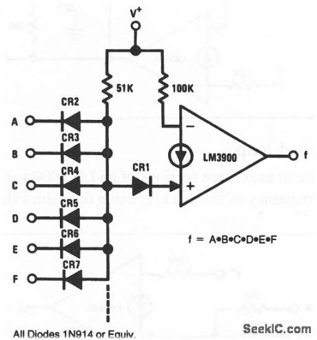
This circuit uses one section of an LM3900 to form a multiple-input AND gate, with an input-diode network that is similar to that of DTL. Interchange the inputs to form a NAND gate. National Semiconductor, Linear Applications Handbook 1991 p 240 (View)
View full Circuit Diagram | Comments | Reading(716)
HYBRID_D_C_OPERATIONAL_AMPLIFIER
Published:2009/7/10 22:02:00 Author:May
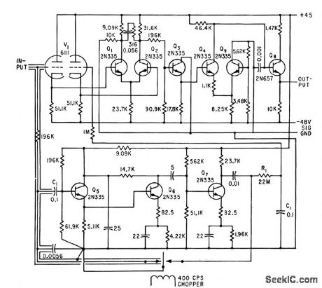
Uses Goldberg chopper-stabilized principle for d-c drift correction. D-c gain is 900,000, input impedance 230,000 ohms, and output impedance 1,000 ohms. Generates -20 to +20v.across 10,000-ohm load at 0 to 800 cps.-R. L.Konigsberg, Designing Hybrid D.C Amplifiers to Withstand Missile Environments, Electronics,34:32, p157-159. (View)
View full Circuit Diagram | Comments | Reading(735)
_5_V_WITH_LM3OOH
Published:2009/7/17 4:40:00 Author:Jessie
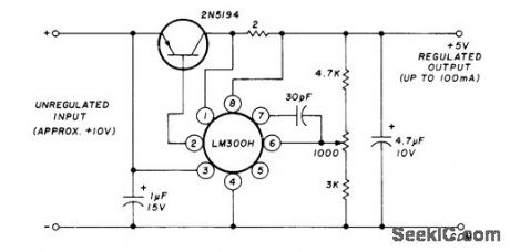
Series power transistor and National IC voltage regulator provide up to 100 mA. Improved version of regulator,LM305H, may be substituted.-H. Olson, Power-Supply Servicing, Ham Radio, Nov.1976, p 44-50. (View)
View full Circuit Diagram | Comments | Reading(1022)
ac_TO_dc_CONVERTER
Published:2009/7/10 22:02:00 Author:May
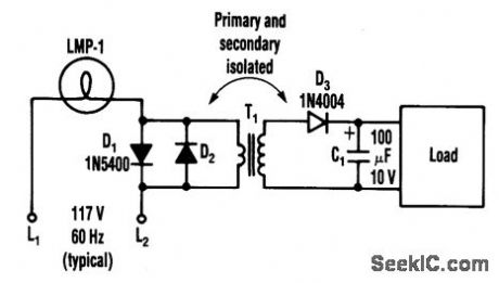
By coupling two back-to-back diodes in series with an ac power circuit, a voltage of about 1.4 Vpp can be obtained. This voltage is useful for exciting the primary coil of a small transformer. The voltage induced in the secondary coil can then be rectified and used to power solid-state control circuits. The forward-voltage drop of the diodes is inherently constant and stable over a wide range of accircuit power variations.The resulting voltage developed across the transformer windings is also free from variation that might be caused by changes in the circuit's current or voltage.
In the circuit, a lamp (LMP-1) is connected to the primary ac input line (L1 and L2) through a pair of inverse-parallel-connected power diodes (D1and D2). As power flows to the lamp, a drop of about 0.7 V is alternatively developed across each of the diodes. This voltage feeds the primary of a small ransformer (T1). T1 can be a small 8-Ω to 500-Ω transistor radio output, etc. This will deliver about 11 Vpp across its secondary winding. LMP1 can be a small 120-V lamp of 5 to 25 W, etc. (View)
View full Circuit Diagram | Comments | Reading(0)
BLOOD_FLOW_CONTROL
Published:2009/7/17 4:40:00 Author:Jessie
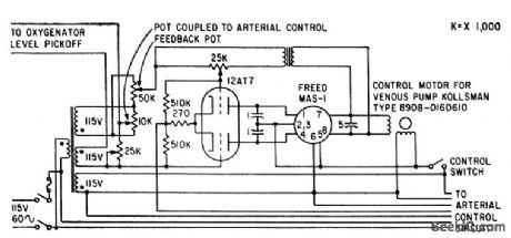
Used to correct long-term differences in flow rates of venous one arterial pumps. Venous control portion of heart-lung amplifier has two inputs, a signal derived from oxygenator level error and an input from potentiometer connected to arterial transmission control lever.-R. Roberts und J. Loeffler, Automatically Controlled Heart-Lung Machine, Electronics, 33:31, p 91-93. (View)
View full Circuit Diagram | Comments | Reading(721)
6_30_V_AT_500_mA
Published:2009/7/17 4:40:00 Author:Jessie
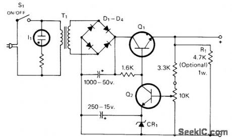
Zener used for CR1 should be rated 1 V less than desired minimum voltage, at 300 mW. R1 improves regulation at low cur rent levels. Current-limiting value is about 1 A. Diodes are 50-PIV 1-A silicon. I1 is 117-V neon lamp, Q1 is any 15-W NPN power transistor. Q2 is 2N697 or equivalent. T1 is power transformer with 24-V secondary at 0.5 A.-J. Huffman, The Li'I Zapper-a Versatile Low Voltage Supply, CQ, Nov. 1977, p 44. (View)
View full Circuit Diagram | Comments | Reading(762)
FOUR_CHANNEL_ADAPTER_FOR_CRO
Published:2009/7/10 22:00:00 Author:May
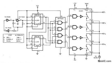
DG201 CMOS analog switch controlled by 50-kHz clock allows display of four input signals simultane-ously on singletrace oscilloscope, Adapter is used in chop mode for signals below 500 Hz. Frequencies above 500 Hz are best viewed in altemate mode with clock frequency of 200 Hz. One of inputs is used to trigger horizontal trace of CRO.- Analog Switches and Their Applications, Siliconix,Santa Clara,CA,1976,p7-63-7-66. (View)
View full Circuit Diagram | Comments | Reading(966)
Video_amplifier_with_AGC_using_an_MC1552
Published:2009/7/17 4:39:00 Author:Jessie
Video amplifier with AGC using an MC1552(courtesy Motorola semiconductor Products Inc.). (View)
View full Circuit Diagram | Comments | Reading(695)
LOW_Z_INPUT
Published:2009/7/10 21:59:00 Author:May
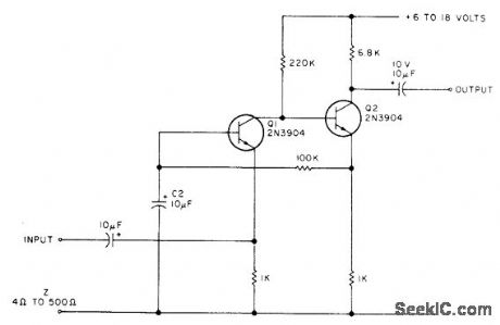
Can be used with low-impedance source, such as 4- to 16-ohm loudspeaker or telephone earphone used as mike. If loudspeaker is put out in yard, sensitivity is sufficient to pick up sounds made by prowlers. Can.be fed into input of any high-fidelity amplifier.-E. Dusina, Build a General Purpose Preamp, 73 Magazine, Nov. 1977, p 98.
(View)
View full Circuit Diagram | Comments | Reading(808)
±7_VDC_OFFSET
Published:2009/7/10 21:58:00 Author:May
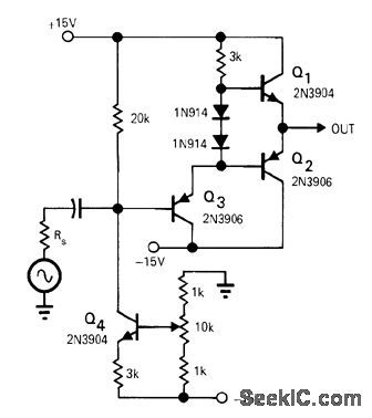
High-impedance current source Q4 provides desired level shiftfor AC signals in video circuit whose DC level controls intensity of CRT. Input and offset signals are fed to base of Q3 which drives complementary-symmetry emitter-follower Q1-Q2. For values shown, level can be shifted about ±7 VOC.-P.B. Uhlenhopp, Variable DC Offset Using a Current Source, EDN|EEE Magazine, Aug. 15, 1971, p46. (View)
View full Circuit Diagram | Comments | Reading(847)
CATHODE_DRIVE_FOR_CRT
Published:2009/7/10 21:57:00 Author:May
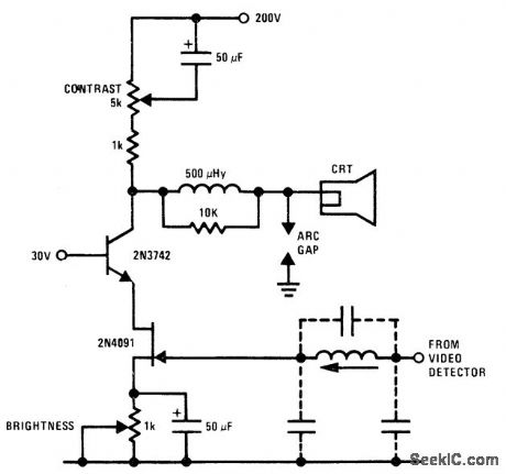
Cascode connection of 2N4091 JFET and 2N3742 bipolar transistor provide full video output for cathode. Gain is about 90. M-derived filter using stray capacitances and variable inductor blocks 4.5-MHz sound frequency from video amplifier. Cascode coAfiguration eliminates Miller capacitance problems of JFET, allowing direct drive from video detector.- FET Databook, Na-tional Semiconductor, Santa Clara, CA, 1977, p 6-26-6-36. (View)
View full Circuit Diagram | Comments | Reading(1109)
COMMUTATOR
Published:2009/7/10 21:57:00 Author:May
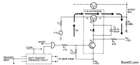
Bipolar pnp trcmsistor, diode, and fet lransislor in basic module form analog switch used as electronic commutator for choppers and telemetry multiplexing.-J, Gulbenk and T. F. Prosser, How Modules Make i Complex Design Simple, Electronics,37:32, p50-54. (View)
View full Circuit Diagram | Comments | Reading(1592)
TELEMONITOR_FOR_RECORDING_PHONE_CALLS
Published:2009/7/10 21:55:00 Author:May
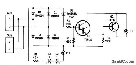
This circuit switches a tape recorder via PL2. When on-hook, D5 conducts, turns on Q1, and cuts off Q2. Ringing voltage will also cause D5 to conduct; C2 and C1 should be rated 150 V or higher. When phone is off-hook, the 10 V or so present on the line will not break down D5, and therefore Q1 is off and Q2 is biased on. PL2 connects to the remote control jack on the tape recorder. Audio is taken from PL1.Caution: Use either a battery tape recorder or an FCC/CSA/UL-approved ac adapter-powered tape recorder. This precaution is to avoid inadvertent 120 Vac on the telephone line. (View)
View full Circuit Diagram | Comments | Reading(865)
SHOCK_SPECTRUM_ANALYZER_WITH_PEAK_VOLTAGE_MEMORY
Published:2009/7/17 4:39:00 Author:Jessie
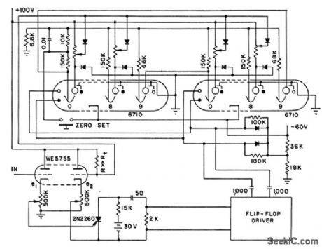
Each peak voltage-memory circuit has frequency-determining L-C filter. Shock spectrum of input pulse is defined by peak voltage across each filter capacitor. Memory is Burroughs Beam-X switching tube in which beam is advanced one position for each voltage increment. Output is d-c voltage suitable for automatic plotting.-Contest Produces Novel Circuit Designs, Electronics, 36:11, p 96-102. (View)
View full Circuit Diagram | Comments | Reading(790)
HIGH_GAIN_INTERCOM
Published:2009/7/10 21:54:00 Author:May
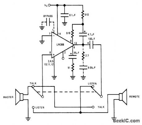
Internal bootstrapping in National LM388 audio power amplifier IC gives output power levels above 1 W at supply voltages in range of 6-12 V, with minimum parts count. AC gain is set at about 300 V/ V, eliminating need for stepup transformer nor mally used in intercoms. Optional RC network suppresses spurious oscillations.- Audip Handbook, National Semiconductor, Santa Clara, CA, 1977, p 4-37-4-41. (View)
View full Circuit Diagram | Comments | Reading(867)
Video_amplifier_using_an_MC1590
Published:2009/7/17 4:39:00 Author:Jessie
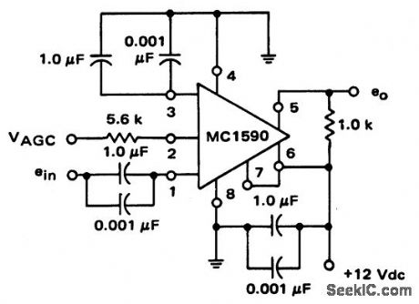
Video amplifier using an MC1590(courtesy Motorola Semiconductor Products Inc.). (View)
View full Circuit Diagram | Comments | Reading(735)
| Pages:801/2234 At 20801802803804805806807808809810811812813814815816817818819820Under 20 |
Circuit Categories
power supply circuit
Amplifier Circuit
Basic Circuit
LED and Light Circuit
Sensor Circuit
Signal Processing
Electrical Equipment Circuit
Control Circuit
Remote Control Circuit
A/D-D/A Converter Circuit
Audio Circuit
Measuring and Test Circuit
Communication Circuit
Computer-Related Circuit
555 Circuit
Automotive Circuit
Repairing Circuit