
Circuit Diagram
Index 814
HIGH_POWER_PULSE_GENERATOR
Published:2009/7/17 5:05:00 Author:Jessie
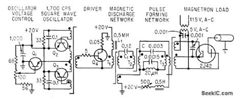
Power transistors and saturable transformers serve in place of hydrogen thyratrons for generating pulses with 1-megawatt peak power for sonar and radar. Low-voltage capacitor is first charged to voltage that is regulated on pulse-to-pulse basis rather than from regulated supply. Capacitor is then discharged through saturable stop-up transformer L1 to charge high-voltage capacitor, which in turn is discharged through magnetron load.-R. T. Maguire, SCR's to Pulse Radar, Electronics, 37:3, p 14-15. (View)
View full Circuit Diagram | Comments | Reading(1520)
Light_operated_relay
Published:2009/7/17 5:04:00 Author:Jessie
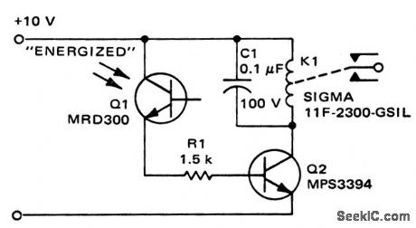
Light-operated relay.The phototransistor can be activated by a flashlight(courtesy Motorola semiconductor Products Inc.). (View)
View full Circuit Diagram | Comments | Reading(1834)
IHREE_FET_A_C_AMPLIFIER
Published:2009/7/10 5:29:00 Author:May
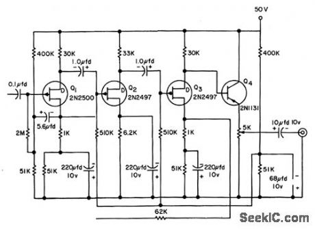
Can be used in applications requiring amplilcation of microvolt signals, as in ultrasensitive preamps for null detectors, medical research equipment, recorders, osciloscopes, and low-level transducers. With 100K generator resistance, amplifier 3-db bandwidth is 1 cps to 40 kc.-L.J. Sevin, Jr., Field-Effect Transislors, McGraw-Hill, N.Y., 1965, p 107.
(View)
View full Circuit Diagram | Comments | Reading(778)
±10V_TRACKING
Published:2009/7/17 5:04:00 Author:Jessie
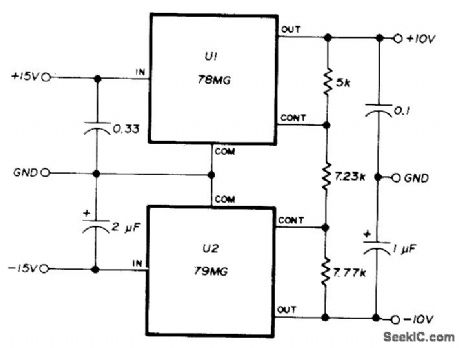
Fairchild 78MG and 79MG positive and negative voltage-regulator ICs pro-vide up to 500-mA output, with protection against short-circuits and thermal overloads.-D. Schmieskors, Adjustable Voltage-Regulator ICs, Ham Radio, Aug. 1975, p 36-38. (View)
View full Circuit Diagram | Comments | Reading(1511)
Photo_activated_logic_driver_1
Published:2009/7/17 5:03:00 Author:Jessie
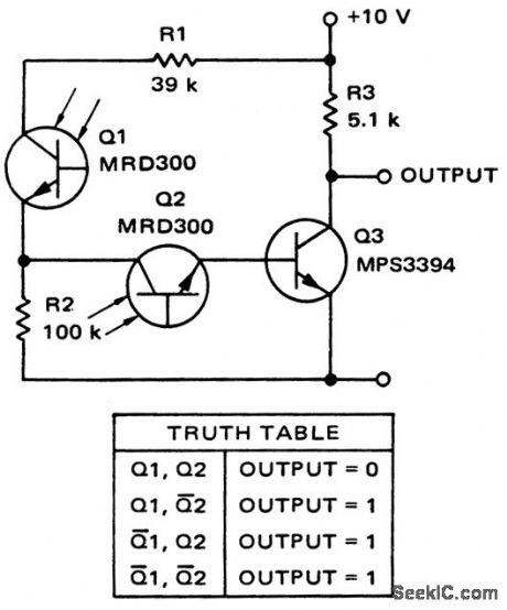
Photo-activated logic driver (courtesy Motorola Semiconductor Products Inc.). (View)
View full Circuit Diagram | Comments | Reading(689)
45_34V_AT_1A
Published:2009/7/17 5:02:00 Author:Jessie
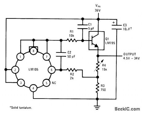
Combination of LM195 power transistor IC and standard LM105 regulator gives better than 2-mV load regulation with overload protection. Differential between input and output voltages is only 2 V.- Linear Applications, Vol. 2, National Semiconductor, Santa Clara, CA, 1976, AN-110, p 4. (View)
View full Circuit Diagram | Comments | Reading(782)
Photo_activated_logic_driver
Published:2009/7/17 5:01:00 Author:Jessie
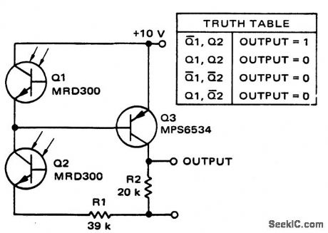
Photo-activated logic driver(courtesy Motorola semiconductor Products Inc.). (View)
View full Circuit Diagram | Comments | Reading(823)
_05_TO_1V_BIAS
Published:2009/7/17 5:00:00 Author:Jessie
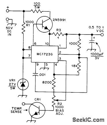
Motorola MC1723G regulator, 2N5991 current-boost transistor, and base-emitter junction of 2N5190 transistor CR1 serve as adjustable bias voltage source for 300-W solid-state power amplifier. R3 sets current limiting at about 0.65 A. Measured output-volt-age variations are about ±6 mV for load changes of 0 to 600 mA, -H. O. Granberg, One KW-Solid-State Style, 0ST, April 1976, p 11-14. (View)
View full Circuit Diagram | Comments | Reading(1462)
0_20_V_CURRENT_LIMITING
Published:2009/7/17 5:00:00 Author:Jessie


Novel full-wave voltage doubler formed by diode bridge and C1-C2-C3 provides 39 V required by μA723 regulator whose output is continuously variable with R1. Initially, R2 is adjusted for minimumoutput voltage when R1 is maximum counterclockwise, to balance bridge R1-R2-R3-R4 when output voltage is zero. Value used for RSC determines short-circuit current. Raw DC supply provides separate 25 V for pass transistors. - L. Drake, Variable Voltage Power Supply Uses Minimum Components, EDN Magazine, Aug. 5, 1974,p 80 and 82.
(View)
View full Circuit Diagram | Comments | Reading(1262)
Norton_low_drift_ramp_and_hold
Published:2009/7/17 4:59:00 Author:Jessie
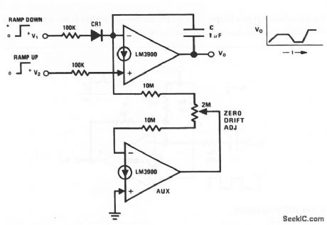
This circuit uses two sections of an LM3900 to form a low-drift ramp-and-hold circuit with a zero-drift adjustment. If both inputs are at zero volts, the circuit is in hold (after proper zero-drift adjustment). Raising either input causes the dc output to ramp up or down, depending on which input goes positive. The ramp slope is a function of the input-voltage magnitude. Additional inputs can be placed in parallel to increase the input-control variables. National Semiconductor, Linear Applications Handbook 1991 p 249 (View)
View full Circuit Diagram | Comments | Reading(867)
_2_TO__35V_AT_10A
Published:2009/7/17 4:58:00 Author:Jessie
Provides fixed output voltage at value determined by choice of resistance values, computed as given in table. Heat-sink should have very low thermal resistance.For similar range of negative voltages, Motorola MPC900 regulator can be used, with circuit modified slightly as set forth in article.-H. Olson, Second-Generation IC Voltage Regulators, Ham Radio, March 1977, p 31-37. (View)
View full Circuit Diagram | Comments | Reading(707)
Light_operated_SCR_alarm_using_a_sensitive_gate_SCR
Published:2009/7/17 4:58:00 Author:Jessie
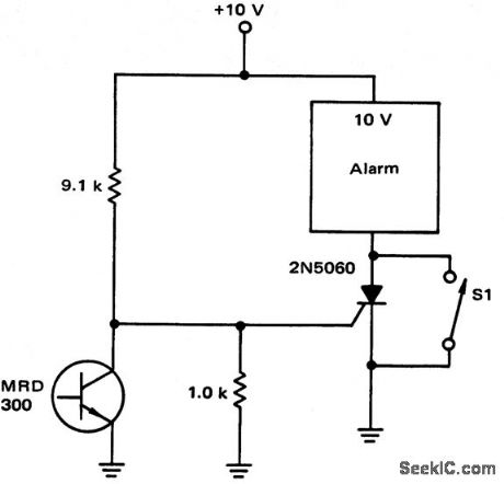
Light-operated SCR alarm using a sensitive gate SCR (courtesy Motorola Semiconductor Products Inc.). (View)
View full Circuit Diagram | Comments | Reading(1101)
Norton_difference_integrator
Published:2009/7/17 4:58:00 Author:Jessie
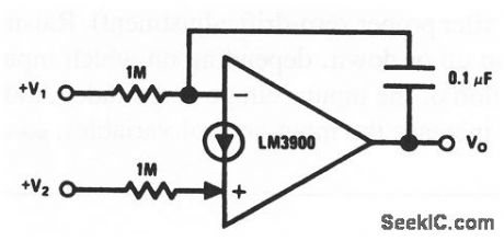
This circuit shows one section of an LM3900 that is used to form a difference integrator. In addition to being the basis for many sweep circuits, this circuit can also provide the time integral of the difference between two input waveforms. This is useful for dc feedback loops because both the comparison to a reference and the integration occur in one amplifier. National Semiconductor linear Applications Handbook 1991 p 248 (View)
View full Circuit Diagram | Comments | Reading(808)
Norton_differentiator
Published:2009/7/17 4:58:00 Author:Jessie
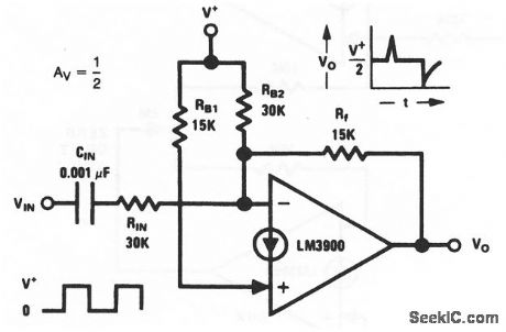
This circuit shows one section of an LM3900 that is used to form a differentiator. Notice that the differentiated output is one-half of the square-wave input. National Semiconductor, Linear Applications Handbook, 1991, p 248 (View)
View full Circuit Diagram | Comments | Reading(678)
Light_relay_operated_SCR_alarm_circuit
Published:2009/7/17 4:57:00 Author:Jessie
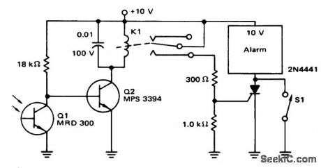
Light-relay-operated SCR alarm circuit(courtesy Motorola Semiconductor Pro-ducts Inc.). (View)
View full Circuit Diagram | Comments | Reading(866)
12_V_AT_28_A
Published:2009/7/17 4:57:00 Author:Jessie
Simple supply was developed for use with 2-meter FM transceiver when operating in home Power transistors are Radio Shack 276-592 rated 40 W. T1 is 12.6 V at 3 A, and U1 is 276-1171 rated 100 V at 6 A. Article covers construction.-M. L. Lovell, 12 Inexpensive Volts for Υour Base Station, 73 Magazine, Sept. 1976, p 60-62. (View)
View full Circuit Diagram | Comments | Reading(735)
Photo_driven_pulse_stretcher
Published:2009/7/17 4:57:00 Author:Jessie
Photo-driven pulse stretcher (courtesy Motorola Semiconductor Products Inc.). (View)
View full Circuit Diagram | Comments | Reading(703)
Battery_operated_fluorescent_light_for_one_or_two_8_watt_units
Published:2009/7/17 4:54:00 Author:Jessie
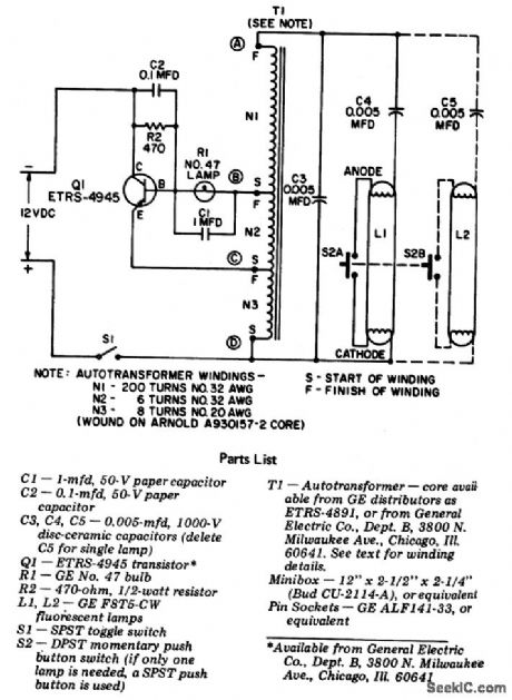
Battery operated fluorescent light for one or two 8-watt units. The circuit is a simple transistor inverter operated by a 12-volt battery. T1 is 200 turns of AWG #32 magnet wire in two layers of 100 turns each. Cover the first layer with electrical tape before starting the second. Then cover the second with tape. Mark the two ends as start (S) and finish (F); mark this winding as N1. Next wind N2 as six turns of AWG #32 magnet wire over N1 in the same direction. Mark each end of N2 with start (S) and finish (F). Then wind N3 as eight turns of AWG #20 magnet wire over N2 in the same direction. Mark N3 with S and F leads. Each layer should have electrical tape over it (courtesy General Electric Company). (View)
View full Circuit Diagram | Comments | Reading(1305)
Norton_squaring_amplifier_with_hysteresis
Published:2009/7/17 4:52:00 Author:Jessie
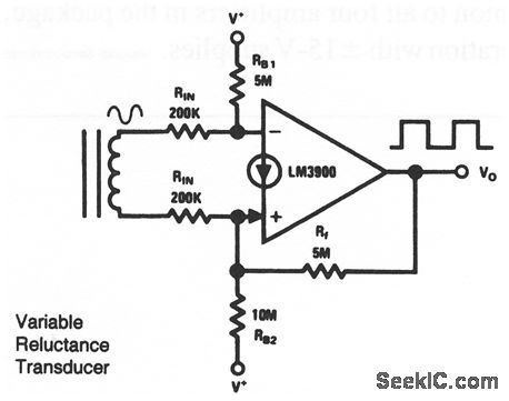
This circuit shows one section of an LM3900 that is used to form a squaring amplifier for use with a variable-reluctance transducer. The circuit produces symmetrical hysteresis above and below the zero-output state (for noise immunity), and filters high-frequency input noise disturbances. With the values shown, the trip voltages are about ±150 mV, centered about the zero-output state of the transducer (at low frequencies where the low-pass filter is not attenuating the input signal). National Semiconductor Linear Applications Handbook, 1991 p 247 (View)
View full Circuit Diagram | Comments | Reading(3510)
Norton_direct_coupled_amplifier_with_±15_V_supplies
Published:2009/7/17 4:52:00 Author:Jessie
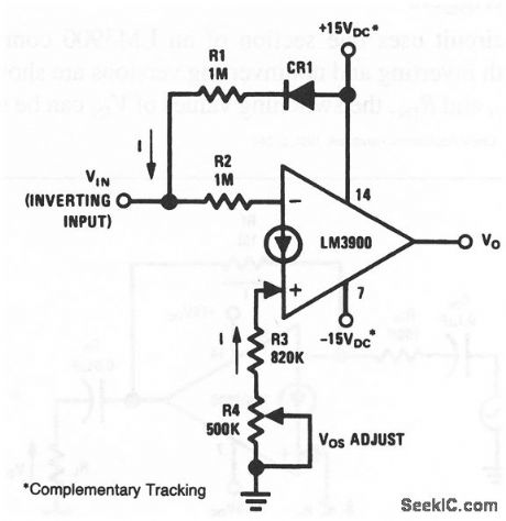
This circuit uses one section of an LM3900 to form a direct-coupled inverting amplifier. The ±15-V supplies must have complementary tracking, and R4 adjust for proper offset (or zero offset) at the output. National semiconductor, Linear Applications Handbook 1991 p 246 (View)
View full Circuit Diagram | Comments | Reading(733)
| Pages:814/2234 At 20801802803804805806807808809810811812813814815816817818819820Under 20 |
Circuit Categories
power supply circuit
Amplifier Circuit
Basic Circuit
LED and Light Circuit
Sensor Circuit
Signal Processing
Electrical Equipment Circuit
Control Circuit
Remote Control Circuit
A/D-D/A Converter Circuit
Audio Circuit
Measuring and Test Circuit
Communication Circuit
Computer-Related Circuit
555 Circuit
Automotive Circuit
Repairing Circuit