
Circuit Diagram
Index 805
SWEEP_GENERATOR
Published:2009/7/17 4:22:00 Author:Jessie
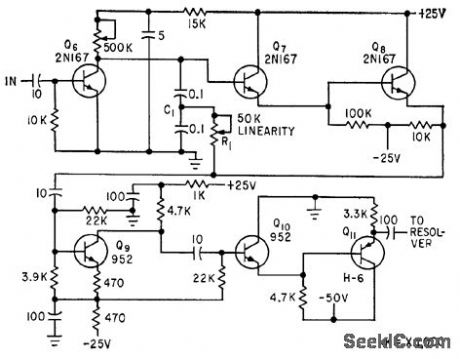
Accepts pulse from monostable mvbr and generates signal for sweep resolver of ppi radar. Voltage rises at constant rate during mono off time, and is held at zero during on time. Cascaded emitter-follower Q7-Q8 provides impedance match to output. Q9-Q10-Q11 provide required power for sweep resolver while preventing thermal runaway at normal temperatures.-C. E. Veazie, Transistorized Radar Sweeps Circuits Using Low Power, Electronics, 32:26, p 46-47. (View)
View full Circuit Diagram | Comments | Reading(2841)
150_MHz_to_300_MHz_frequency_doubler_using_an_MC1596G
Published:2009/7/17 4:21:00 Author:Jessie
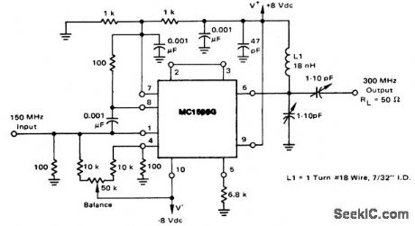
150 MHz to 300 MHz frequency doubler using an MC1596G. Spurious outputs are 20 dB below the desired output (courtesy Motorola Semiconductor Products Inc.). (View)
View full Circuit Diagram | Comments | Reading(701)
Low_frequency_doubler_using_an_MC1596G
Published:2009/7/17 4:20:00 Author:Jessie
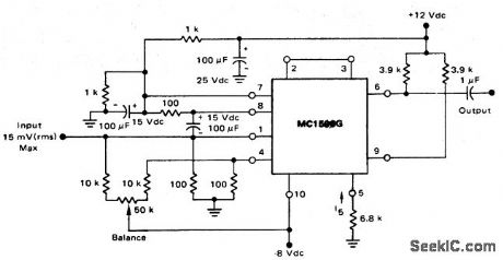
Low-frequency doubler using an MC1596G. This circuit works well in the low-frequency and audio range below 1 MHz (courtesy Motorola Semiconductor Products Inc.). (View)
View full Circuit Diagram | Comments | Reading(829)
Norton_direct_coupled_power_amplifier
Published:2009/7/17 4:20:00 Author:Jessie

This circuit uses one section of an LM3900 and a Darlington pair to provide an output of 3 A into the load. National Semiconductor Linear Applications Handbook 1991, p 223 (View)
View full Circuit Diagram | Comments | Reading(883)
Frequency_doubler
Published:2009/7/17 4:20:00 Author:Jessie
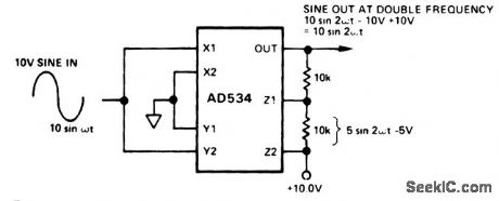
Frequency doubler. This circuit accepts a sinusoidal signal with a 10-voh amplitude and produces a double-frequency signal also having a 10-volt amplitude with no DC offset (courtesy Analog Devices, Inc.). (View)
View full Circuit Diagram | Comments | Reading(0)
00001_TO_1_μF_IN_F0UR_RANGES
Published:2009/7/10 21:29:00 Author:May
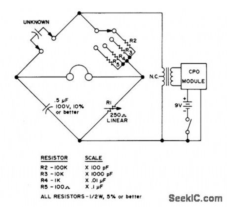
SimpIe bridge uses AF voltage from Cordover CPO-4 code practice oscillator module, fed through transistor output transformer connected in reverse for impedance matching. Earphones serve as null detector, but amplifier can be added for greater sensitivity or CRO used. Only one scale need be calibrated, using known values of capacitors.-W. P. Tumer, Build a Basic Bridge, 73Magazine, Nov. 1974, p 95. (View)
View full Circuit Diagram | Comments | Reading(611)
2_W_LM380_POWER_AMPLIFIER
Published:2009/7/10 21:28:00 Author:May
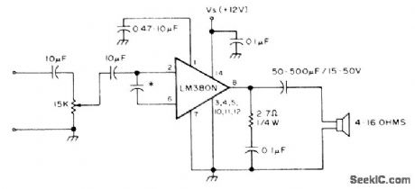
Complete basic circuit for most audio or communication purposes uses minimum of extemal parts. C3, used to limit high frequencies, can be in range of 0.005 to 0.05 F.-A. MacLean, How Do You Use ICs?, 73 Magazine, June 1977, p 184-187. (View)
View full Circuit Diagram | Comments | Reading(791)
AUDIO_POWERED_TAPE_RECORDER_CONTROLLER
Published:2009/7/10 21:26:00 Author:May
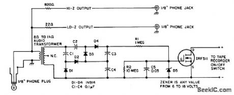
A tape recorder can be controlled by rectifying the audio input and driving an IRF511 power MOSFET to switch a tape recorder on when audio is present. This circuit was used with a communications receiver to record intermittent transmissions (such as aircraft, repeater output. etc.). (View)
View full Circuit Diagram | Comments | Reading(838)
ELECTROLYTICS_WITH_REFORMING
Published:2009/7/10 21:24:00 Author:May
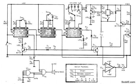
Automatic tester for electrolytics applies voltage for about 15 s to repolarize dielectric before measurement is made. This provides sufficient reforming for test purposes, using 12 V through 1200 ohms, but test should be repeated if leakage current is high because of incomplete re forming. Tone from loudspeaker indicates end of 15-s reforming period. Green LED, indicates reforming process is readyto start. Red LED, indicates excessive current is flowing during reforming. LED, flashes to indicate test capacitor is being charged during measuring cycle. Article covers construction and calibration in detail. IC, is SN74123N, IC, is SN74121N, and IC, is SN7413N.-A. Drummond-Murray, Electrolytic Capacitor Tester, Wireless World, May 1977, p 47-49. (View)
View full Circuit Diagram | Comments | Reading(1632)
TEMPERATURE_TO_PULSE_WIDTH
Published:2009/7/10 21:24:00 Author:May
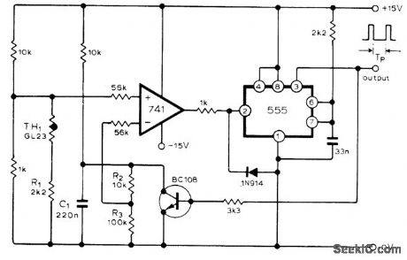
Temperature-dependent current through thermistor TH1 develops voltage across R1 that is compared with fraction of increasing voltage across C1 by 741 opamp. When output of opamp goes negative, it triggers 555 IC connected as mono MVBR, to turn transistor on for about 100 μs and discharge C1. Circuit is based on similarity between resistan ce-tem peratu re curve of ther-mistor and inverse function of voltage across capacitor charging through resistor. For values shown, circuh gives 650-μs pulse width at 0℃, increasing 20 μs per degree with accuracy of ±1.2℃ up to 60℃. If IC output is used to gate clock oscillator, number of oscillator output pulses will be directly proportional to temperature.-T. P. Y. Sander, Temperature to PulseLength Converter, Wireless World, Jan. 1977, p 76. (View)
View full Circuit Diagram | Comments | Reading(1539)
NOVEL_METRONOME
Published:2009/7/10 21:23:00 Author:May
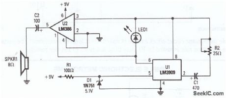


The LM3909 is conftgured so that the frequency of oscillation is dependent on a single RC timing circuit, which consists of C1 and R2. LED1 discharges capacitor C1 and the resultant pulse is directed into pin 3 as well as pin 1 of the LM386 audio amplifier to extemally control that unit, thereby providing ade-quate volume. The circuit, as it is configured, provides frequency ranges from 57 to 204 beats per minute, and plenty of volume. (View)
View full Circuit Diagram | Comments | Reading(737)
±5_V_AND_±12_V
Published:2009/7/17 4:19:00 Author:Jessie

Four different National voltage regulators provide voltages required for wide-range function generator. Power transformer is Triad F90X. - R. C. Dobkin, Wide Range Function Generator, National Semiconductor, Santa Clara, CA, 1974, AN-115. (View)
View full Circuit Diagram | Comments | Reading(685)
PERFECT_CAPACITOR
Published:2009/7/10 21:22:00 Author:May
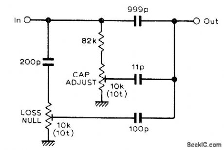
Simple circuit shown provides equivalent of perfect no-loss 1000-pF capacitor at frequencies below about 100 kHz.Principle can be used to construct fixed-fre-quency capacitance standards for use in high-accuracy capacitor bridge. All capacitors are silver mica. If mounted in oven, stability can be 1 PPM and residual phase-angle difference from pure capacitance only 1 microradian.-B. J.Frost, No Loss Capacitor, Wireless World, Dec. 1977, p 80. (View)
View full Circuit Diagram | Comments | Reading(1060)
Norton_amplifier_with_zero_volts_out_for_zero_volts_in_
Published:2009/7/17 4:19:00 Author:Jessie
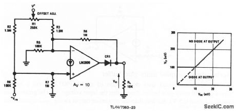
This circuit uses one section or an LM3900 to form a noninverting direct-coupled amplifier, where zero volts input produces zero volts output. Figure 11-39B shows the voltage transfer function for the circuit, both with and without diode CR1 at the output. National Semiconductor Linear Applications Handbook, 1991 p. 222, 223 (View)
View full Circuit Diagram | Comments | Reading(728)
TRANSISTOR_TURNS_OP_AMP_ON_OR_OFF
Published:2009/7/10 21:22:00 Author:May
When transistor Q1 is switched off, the circuit behaves as a voltage follower. By applying a positive voltage to the emitter of Q1 via a 10 Ω resistor, the transistor is made to turn on and go into saturation. Thus, the lower end of R4 is connected to ground. The circuit has not changed into that of a differential amplifier, except that the voltage difference is always 0 V As long as the resistor ratios in the two branches around the op amp are in the same ratio, the output should be zero. A 47-kΩ resistor is used to null out any ratio errors so that the OFF attenuation is more than 60 dB. The high common-mode rejection ratio of a 741 enables this large attenuation to be obtained. (View)
View full Circuit Diagram | Comments | Reading(787)
DISTANCE_MARK_GENERATOR
Published:2009/7/17 4:19:00 Author:Jessie
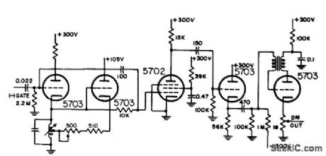
Uses switched Hartley oscillator, pentode amplifier-shaper, and series-triggered blocking oscillator to generate 20-mile distance marks in airborne search radar.-NBS, Handbook Preferred Circuits Navy Aeronautical Electronic Equipment, Vol. 1, Electron Tube Circuits, 1963, p N8-2. (View)
View full Circuit Diagram | Comments | Reading(666)
PLL_CAPACITANCE_METER
Published:2009/7/10 21:22:00 Author:May
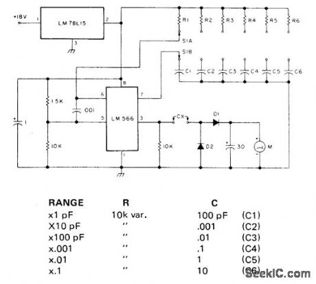
Based on fact thatalternating cument floating through capacitordepends on applied voltage, frequency,and capacitance value Circuit uses square wave forcharging capacitor to full voltage,then measures current flow as linear function of capacitance,LM78L15 provides regulated 15 V for LM566 PLL VCO. Frequency ofVCO depends on values of R and C selected by rotary switch S1,to give six linear scales:0-10 pF.10-100 pF.100-1000 pF,1000 pF to 0.01 μF,0.01-0.1μF and 0.1-1 μF Accuracy is about±5% Meter is 100 μA.Use small signal diodes,-S.Shields,How Many pF is That Capacitor,Really?, 73 Mgazine, March 1978,p 48-50.
(View)
View full Circuit Diagram | Comments | Reading(1784)
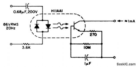
HYBRID_30_MC_I_F
Published:2009/7/17 4:18:00 Author:Jessie
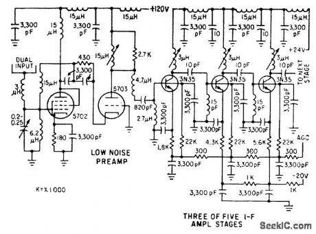
Bandwidth is 6 Mc, noise figure is below 2.5 db, and gain is enough to give 1 V peak-to-peak noise output into 1,000-ohm load when using two transistorzed video stages following the five transistorized i-f gain stages.-J. Scott, D. Randise, and R. P. Lukacovic, Portable Radar Traces Battlefield Deployment, Electronics, 33:12, p 67-70. (View)
View full Circuit Diagram | Comments | Reading(697)
THERMOMETER
Published:2009/7/10 21:21:00 Author:May
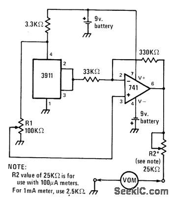
Sensor is 3911 ICwhoseout-put is 10 mV/K (kelvin temperature scale). At 0℃, output is 2.73 V. Output swing is amplified by 741 opamp to 0.1 V/℃ for driving volt-ohm-milliammeter or sensitive milliammeter. R2 ad-iusts scaling factor, for readout in ℃ or °F as de-sired.-J. Sandier, 9 Projects under $9, Modern Electronics, Sept. 1978, p 35-39. (View)
View full Circuit Diagram | Comments | Reading(864)
Norton_line_receiver_amplifier
Published:2009/7/17 4:17:00 Author:Jessie
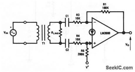
This circuit uses one section of an LM3900 to form a line-receiver amplifier. The use of both inputs cancels out any common-mode signals. The line is terminated by RLINE and the large input impedance of the amplifier does not affect this matched loading. National Semiconductor Linear Applications Handbook 1991 p 221 (View)
View full Circuit Diagram | Comments | Reading(730)
| Pages:805/2234 At 20801802803804805806807808809810811812813814815816817818819820Under 20 |
Circuit Categories
power supply circuit
Amplifier Circuit
Basic Circuit
LED and Light Circuit
Sensor Circuit
Signal Processing
Electrical Equipment Circuit
Control Circuit
Remote Control Circuit
A/D-D/A Converter Circuit
Audio Circuit
Measuring and Test Circuit
Communication Circuit
Computer-Related Circuit
555 Circuit
Automotive Circuit
Repairing Circuit