
Circuit Diagram
Index 807
LINEAR_SCALE
Published:2009/7/10 21:11:00 Author:May
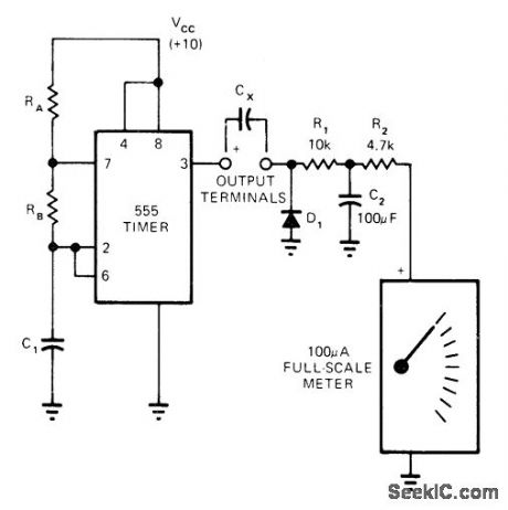
Wide frequency range and high output current of 555 timer contribute to linearity of operation as capacitance meter.Timer is connected as astable MVBR with frequency determined by values used for RA, RB, and C1. When timer output is high, unknown capacitance C1, is charged almost to VCC. When timer goes low, Cx discharges through D1. Use 100 kHz for 100-pF full-scale reading, 10kHz for 1 nF, 1 kHz for 10 nF, and down to 1 Hz for 10μF. Use regulated supply.-R. Horton, 555 Timer Makes Simple Capacitance Meter, EDN Magazine, Nov. 5, 1973, p 81. (View)
View full Circuit Diagram | Comments | Reading(6945)
ACOUSTIC_SOUND_TRANSMITTER
Published:2009/7/10 21:10:00 Author:May
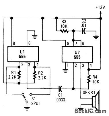
Pulsed sound is produced by this circuit. U1 is used as a bistable multivibrator, which acts as a contact debouncer for S1. C1 feeds a trigger pulse to U2, which feeds apulse to SPKR1, to piezo transducer.Values are shown for a pulse width of 110 μs. (View)
View full Circuit Diagram | Comments | Reading(1174)
MONO_AUDIO_LEVEL_METER
Published:2009/7/10 21:08:00 Author:May

This mono indicator uses both halves of a Samsung KAA2283.Levels displayes are -18 to 0dB in 2-dB steps. Sensitivity is 0.1 to 0.9mV. (View)
View full Circuit Diagram | Comments | Reading(937)
STEREO_AUDIO_LEVEL_METER
Published:2009/7/10 21:07:00 Author:May
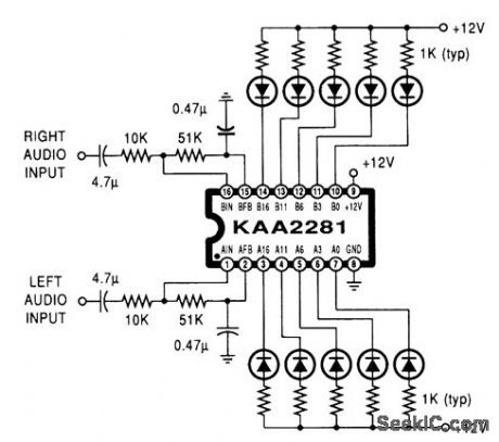
A Samsung KAA2281 and a few LEDs make up a simple stereo indicator. Levels displayed are -16, -11, -6, -3, and 0 dB. Input sensitivity is 1mV. LEDs can be any suitable types or a bar-graph display. (View)
View full Circuit Diagram | Comments | Reading(1905)
3_1_2_digit_LCD_DPM_DVM_using_the_8052_7101_A_D_pair_
Published:2009/7/19 20:46:00 Author:Jessie

31/2-digit LCD DPM/DVM using the 8052/7101 A/D pair (courtesy Intersell, Inc.). (View)
View full Circuit Diagram | Comments | Reading(2056)
INEXPENSIVE_VHF_UHF_DIODE_PF_SWITCH
Published:2009/7/10 21:06:00 Author:May
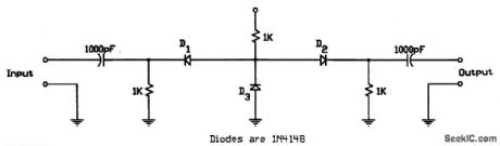
This circuit uses low-cost IN4148 diodes and exhibits about 1.5 dB insertion loss from 10 to 1000 MHz with a few volts of negative bias. D3 conducts and D1/D2 are cut off, which results in 30 to 50 dB isolation. When a few volts of positive bias are applied, D1 and D2 are biased on and D3 is cut off. This circuit should be useful in applications where a low-cost RF switch is necessary. (View)
View full Circuit Diagram | Comments | Reading(742)
0_T0_±15V_INDEPENDENTLY_VARIABLE
Published:2009/7/19 20:45:00 Author:Jessie
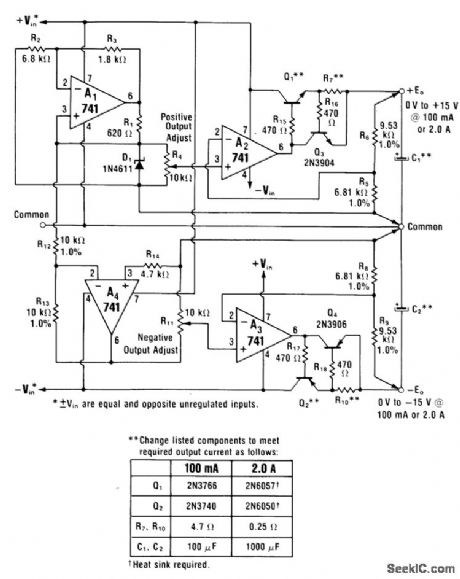
Common zener reference selrves for both regulators. Buffer A3 uses negative reference voltage developed from 6.6-V positive voltage across D1 by inverter A4. Both regulators provide 100mA or 2 A depending on transistors used.-W. G.Jung, IC Op-Amp Cookbook, Howard W. Sams, Indianapolis, IN, 1974, p t62-164. (View)
View full Circuit Diagram | Comments | Reading(767)
R_AND_C_ADAPTEB_FOR_DVM
Published:2009/7/10 21:05:00 Author:May
Self-contained circuit provides four ranges of capacitance (0-1, 10, 100, and 1000 μF) and four ranges of resistance (0-1, 10, 100, and 1000 kilohms) when used with QST combination digital voltmeter and frequency counter. Auxiliary range posilions on switches are provided for special measuring requirements such as temperature sensing, antenna elevation indication, and raingage measurements. For capacitors, constant-current source Q1 charges capacitor linearly.When charging voltage makes U1A switch from positive to negative,C2 stops charging Voltage across C2,proportional tovalue of unknown C2, is then fed to DVM, Article covers construction and calibration.-R Shriner,New Tasks for the Digital Voltmeter,QST,,March 1978,p 19-22. (View)
View full Circuit Diagram | Comments | Reading(752)
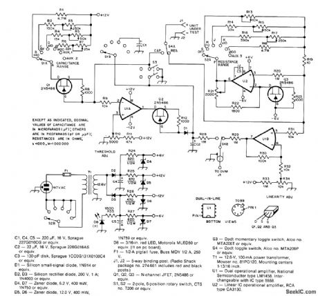
Inexpensive_capacitance_meter
Published:2009/7/19 20:44:00 Author:Jessie
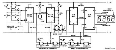
Inexpensive capacitance meter.This circuit uses two 555 timers, or one 556, to generate a gated count for an ICM7217, dependent on the value of capacitance The clock timer operates as a fixed oscillator whose output period is determined by R1, R2 and C. The gating timer also operates as an oscillator, but its output high time is determined by the value of measured capacitance in combination with R3 and R4. Range A reads 1 to 9999 pF, range B reads 1 to 9999 nF, and range B reads 1 to 9999 μF(courtesy Intersil, Inc.). (View)
View full Circuit Diagram | Comments | Reading(5145)
2_35V_VARIABLE
Published:2009/7/19 20:43:00 Author:Jessie
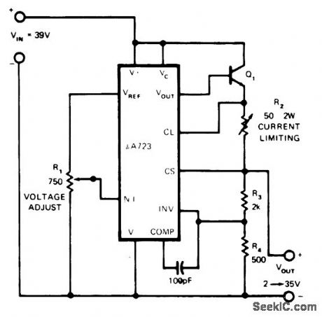
Wide voltage range is achieved by using μA723 regulator IC in simple feedback arrangement requiring only single pot to vary output voltage continuously and linearly from 2 to 35V. Resistors R3 and R4, divide output voltage by 5, so inverting input of regulator sees one-fifth of output voltage. R1 is connected between 7-V reference ofIC and ground to present any intermediate voltage to noninverting input. IC acts to keep these two voltages equal. Maximum input voltage limit is 40V; if possibility of higher voltages exists in lab applications, protect IC with 40-V zener across it.-J. Gangi, Continuously Variable Voltage Regulator, EDN Magazine, Feb. 20, 1973, p 91. (View)
View full Circuit Diagram | Comments | Reading(834)
CHECKING_BY_SUBSTITUTION
Published:2009/7/10 21:04:00 Author:May
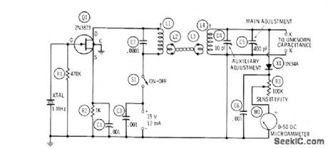
Uses 1-MHz crystal oscillator with fixed-tuned tank circuit L1-C2 link-coupled to resonant measuring circuit consisting of L4, C4, C5, and unknown capacitance. Simple RF voltmeter is connected across measuring circuit as resonance indicator. 04 and C5 have calibrated dials reading directly in picofarads. L1 is Miller 20A224RBI slugtuned unit adjusted to 250 μH. L4 is Miller 41A685CBI adjusted to 60 pH. Links L2 and L3 are 2turnseachJfo use, close S1, set C5 to maximum, and adjust C4 for peak deflection of Ma.Connect unknown capacitance to XX with shortest possible leads, retune CS to resonance, then subtract this capacitance reading of C5 from maximum reading to get value of un known capacitor.-R. P. Tumer, FET Circuits, Howard W.Sams, Indianapolis, IN, 1977,2nd Ed,p 140-142. (View)
View full Circuit Diagram | Comments | Reading(859)
Flowmeter_circuit_for_measuring_the_flow_rate_of_liquids_flowing_at_slow_speeds
Published:2009/7/19 20:42:00 Author:Jessie
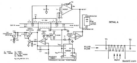
Flowmeter circuit for measuring the flow rate of liquids flowing at slow speeds. To understand the principle of operation refer to Detail A. T1 and T2 are temperature sensors. With no flow through the pipe power is dissipated into the medium symmetrically and there is no difference in temperature at T1 and T2. As flow begins T1 will take on the temperature upstream, but T2 will be influenced by the power dissipated into the moving stream. The time response of the flowmeter is in the order of 10 to 15 seconds (courtesy Analog Devices, Inc.). (View)
View full Circuit Diagram | Comments | Reading(1618)
AUDIO_FILTER_ANALYZER
Published:2009/7/10 21:03:00 Author:May
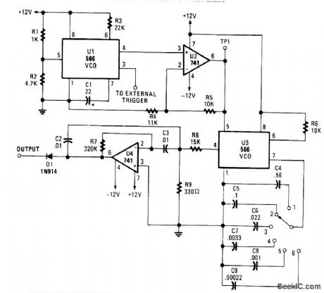
When this circuit is connected to a filter and an oscilloscope, the scope displays the ftlter's frequency response. A frequency that sweeps from low to high is applied to a filter. An oscilloscope is triggered by the start of the sweep and ends its trace at the highest frequency of the sweep. The ftlter output goes to the vertical amplifier of the oscilloscope. Using bandpass filters as an example, as the bandpass frequency is approached, reached, and paqsed, the scope follows the peaking output and draws the response curve.A neat effect!
The 566 VCO (U1) produces a VLF triangle wave to frequency modulate the next stage. It also pro-duces a square wave to externally trigger the scope. Op amp U2 (a 741 unit) optimizes the amplitude and the dc component. Another VCO (U3) produces the actual sweeping triangle wave. Its frequency is select-able via S1. Op amp U4 (another 741 op amp) is set up as a bandpass ftlter and has been included as an example filter. Finally, diode D1 chops off the bottom half of the output, and leaves a nice bell curve.
To set up and operate, power-up the circuit and scope. Set the scope's TIME/CM to 50 ms/cm. Set the VOLTS/CM control to 2V. Attach a probe from the circuit's trigger to the scope's external trigger input. Set the triggering mode to normal, external. Attach a probe from the vertical amplifier to TP1. You'll see a diagonal line that nms across the CRT. Input coupling should be set to dc. Adjust the triggering level until the diagonal runs from the upper left to the lower right of the CRT to ensure a displayed sweep from low to high. Now, disconnect the probe from TP1 and attach it to the filter output past the diode. (View)
View full Circuit Diagram | Comments | Reading(1382)
NARROW_BAND_BALANCED_MODULATOR
Published:2009/7/19 20:40:00 Author:Jessie
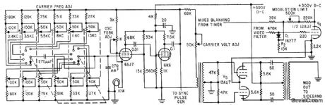
Yields two sidebands and carrier while balancing out original video signal. Gang switch permits use of six different carrier frequencies if sufficient telephone-line band-width is available. Sideband fillers remove upper sideband and part of carrier to provide vestigial sideband operation.-H. W. Gates and A. G. Gatfield, Scan Converter Aids Phone-Line Radar Relay, Electronics, 32:16, p 48-51. (View)
View full Circuit Diagram | Comments | Reading(722)
SWITCHING_CIRCUIT
Published:2009/7/10 20:57:00 Author:May

This switching circuit acts like a bank of interlocked mechanical switches; pushing one of the buttons latches its corresponding output and unlatches a previously selected output. A pair of inverters forms a latch for each output.Pressing button B1, for example, applies a positive pulse, via resistor diode D1B, to the input of the first output's, 0UT1, latch. This positive pulse will set OUT1 high. Feedback locks OUT1's pair of converters in this HIGH state. Meanwhile, the pulse will also pass through diode D1A to the differentiator that is formed by C and R2. The differentiator will shorten the pulse.The shortened pulse goes to all the latches and resets all of them, except the latch that sees the longer setting pulse. Obviously, if you press more than one button at once, more than one output will latch at once. (View)
View full Circuit Diagram | Comments | Reading(1259)
DIFFERENTIAL_TH_ERMOMETER
Published:2009/7/10 20:56:00 Author:May
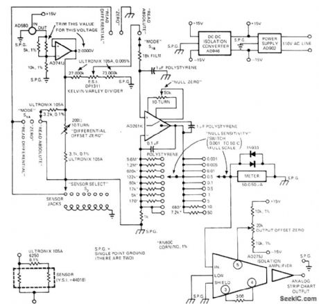
Temperatu re is directly dialed out on five-decade Kelvin-Varley voltage divider, and differences between dialed temperature and that of YS144018 sensor are read directly on meter. Full-seale sensitivity of meter is varied from 0.001 to 50℃ by adjusting gain of AD261K chopper-stabilized null detectorwhich drives both meter and AD275J isolation amplifier used to drive strip-chart recorder. Circuit can also be used to measure temperature difference between two sensors with 100-microdegree accuracy. Article describes other measuring modes as well, includ-ing techniques for measuring 200-nanodegree temperature shifts.-J. Williams, Designer's Guide to: Temperature Measurement, EDN Magazine, May 20, 1977, p 71-77. (View)
View full Circuit Diagram | Comments | Reading(1218)
Component_sorter_of_resistors_capacitors_and_zeners
Published:2009/7/19 20:40:00 Author:Jessie
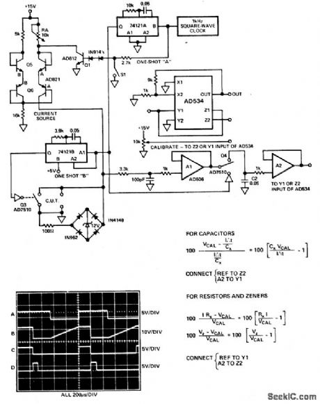
Component sorter of resistors, capacitors, and zeners. Trace A is a 1 kHz square-wave clock that is applied to Q1. The component under test (CUT) in this case is a 0.01 μF capacitor. It is allowed to charge until the clock goes high, turning of the current source (trace B). The voltage the capacitor sits at is inversely proportional to its absolute value. The AD506 follows this potential and feeds the sample-and-hold circuit Q4-C2-A2. The sample-and-hold circuit is enabled by one-shot A for 200 μs when the clock goes high (trace C). After this time one-shot A goes low triggering one-shot B on for 100 μs. This pulse drives Q3 on (trace D) and discharges the CUT. This same fixture can check resistors and zeners by closing S1. This allows the current source to run all of the time. This is necessary since resistors and zeners have no memory (courtesy Analog Devices, Inc.). (View)
View full Circuit Diagram | Comments | Reading(984)
NOISE_GENERATOR
Published:2009/7/10 20:55:00 Author:May
This noise generator provides constant noise energy over its bandwidth, which results from the non-linear behavior of its switching components, more particularly T4. It is very useful for measurements where limited noise bands are required. Varying the ratio R6:R7 and the clock frequency enables the gen-erated noise to be adapted to specific requirements.
Transistors T2 and T3 are current sources. The current through T2 is about 10 times the level of that through T3. Assuming that T4 is on and that the clock input is low, T1 is off, and C2 discharges. The capacitor is pulled to about half of the supply voltage by the two current sources. When that state is reached, stability ensues because the potential then present at the gate of T4 keeps the FET switched on.
When the clock goes high, T1 is switched on so that C2 is connected between the gate of T4 and the earth. Because C2 is only partly charged, the FET is switched off. Transistor T1 is kept switched on by OR gate D1/D2 so that the clock pulses are blocked. Capacitor C2 then charges via T3 until the potential across it becomes high enough to switch on T4. Transistor T1 is then switched off and the circuit is ready to receive another clock pulse (or rather a leading edge of one).
Because it is not known when the clock pulse arrives, it is not known to what potential C2 will be discharged by T2 (and countered by T3). It is therefore also not known when the next clock pulse will arrive. In other words, the pulse width of the output signal is varying constantly, which is characteristic of a noise signal. (View)
View full Circuit Diagram | Comments | Reading(0)
±5V_AT_10_A_WITH_FOLDBACK_CURRENT_LIMITING
Published:2009/7/19 20:38:00 Author:Jessie
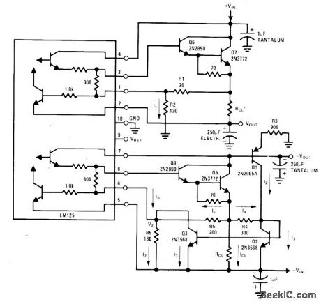
Combination of Darlington pass transistors and current limiting is used with National LM125 dual tracking regulator to give high output currents with protection from short-circuits.-T. Smathers and N. Sevasto-poulos, LM125/LM126/LW127 Precision Dual Tracking Regulators, National Semiconductor, Santa Clara, CA, 1974, AN-82, p 11. (View)
View full Circuit Diagram | Comments | Reading(978)
DISTANCE_MARK_GENERATOR_6
Published:2009/7/19 20:34:00 Author:Jessie
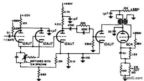
Uses switched Hartley oscillator, monostable mvbr-type trigger shaper, and parallel-triggered blocking oscillator lo generate distance marks for 2, 5, and 25 miles in airborne search radar. RLC unit is switched to change mark spacing.-NBS, Handbook Preferred Circuits Navy Aeronautical Electronic Equipment, Vol. 1, Electron Tube Circuits, 1963, p N8-1. (View)
View full Circuit Diagram | Comments | Reading(688)
| Pages:807/2234 At 20801802803804805806807808809810811812813814815816817818819820Under 20 |
Circuit Categories
power supply circuit
Amplifier Circuit
Basic Circuit
LED and Light Circuit
Sensor Circuit
Signal Processing
Electrical Equipment Circuit
Control Circuit
Remote Control Circuit
A/D-D/A Converter Circuit
Audio Circuit
Measuring and Test Circuit
Communication Circuit
Computer-Related Circuit
555 Circuit
Automotive Circuit
Repairing Circuit