
Circuit Diagram
Index 812
AM_BROADCAS_BAND_SIGNAL_GENERATOR
Published:2009/7/10 5:50:00 Author:May
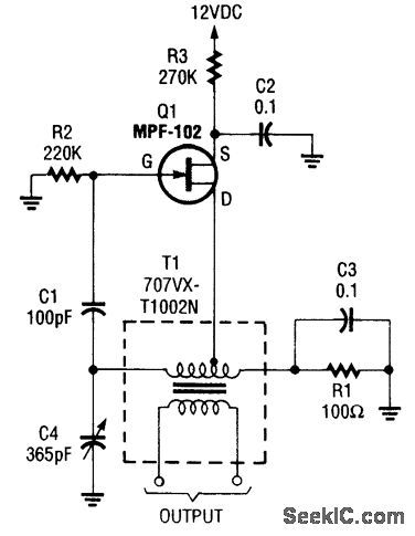
A Hartley oscillator usmg an MPF102 covers the band from 530 to 1600 kHz.T1 is a Toko P/N T1-707VXT1002N 217μhy transformer. (View)
View full Circuit Diagram | Comments | Reading(775)
Photo_activated_logic_driver_3
Published:2009/7/17 5:15:00 Author:Jessie
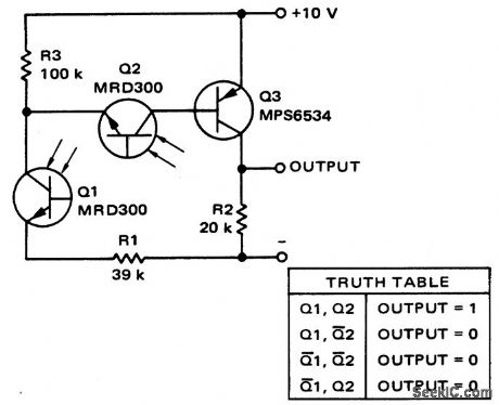
Photo-activated logic driver (courtesy Motorola Semiconductor Products Inc.). (View)
View full Circuit Diagram | Comments | Reading(647)
STEPS_FOR_CURVE_TRACER
Published:2009/7/10 5:49:00 Author:May
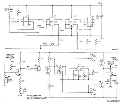
Square waves with 1-V amplitude and 1/60-s period, 2 V at 1/30-s, and 4 V at 11-15 s are generated by μL914 MVBR and μL923 flip-flops U2-U4, for combining in simple ladder network to give staircase waveform. Flip-flops count down MVBR output. Complementary-amplifier stage Q10-Q11 drives phase splitter Q12. Output of phase splitter goes through S1 to appropriate current source, Q13-Q14 or Q15-Q16, for supplying base terminal of device under test (DUT). Use 2N3904 for Q10, Q12, Q15, and Q16. Use 2N3906 for Q11, Q13, and Q14,-R. P. Ulrich, A Semiconductor Curve Tracer for the Amateur, QST, Aug. 1971, p 24-28. (View)
View full Circuit Diagram | Comments | Reading(1729)
STAIRCASE_USES_THREE_OPAMPS
Published:2009/7/10 5:47:00 Author:May
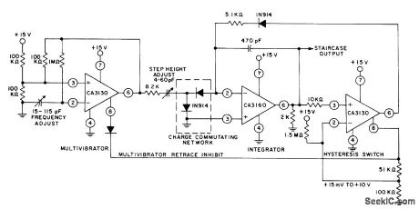
Two CA3130 bipolar MOS opamps serve as multivibrator and hysteresis switch, while CA3160 is connected to generate linear staircase wave-form.- Circuit Ideas for RCA Linear ICs, RCA Solid State Division, Somerville, NJ, 1977, p 6. (View)
View full Circuit Diagram | Comments | Reading(785)
ELECTRONIC_SWITCH_FOR_RADAR_INDICA_TOR
Published:2009/7/17 5:15:00 Author:Jessie
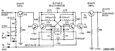
Used to produce aircraft identification markers on ppi. Coincidence of binary voltages supplies gating signals for switch.-J. B. Beach, Coincidence Diodes Gate Electronic Switch, Electronics, 32:8, p 66-68. (View)
View full Circuit Diagram | Comments | Reading(613)
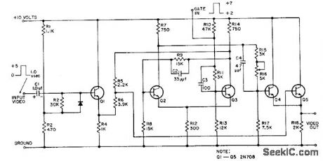
SIX_STEP_COMPOSITE_VIDEO
Published:2009/7/10 5:46:00 Author:May
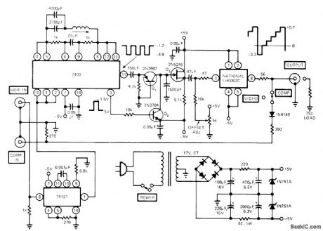
Circuit accepts negatively referenced output signals of TV sync generator and delivers 1 V P-P six-step composite video signal to 75-ohm load. 74121 mono changes wide horizontal blanking pulse to correct width for triggering oscillator IC. National LH002C current driver provides low-impedance drive capability for video signal. Used in testing TV sets and VTR decks.-M. J. Salvati, VFO Adds Versatility to TV Sync Generator, EDN Magazine, May 20, 1974, p 70 and 72. (View)
View full Circuit Diagram | Comments | Reading(3683)
Photo_activated_logic_driver_2
Published:2009/7/17 5:14:00 Author:Jessie
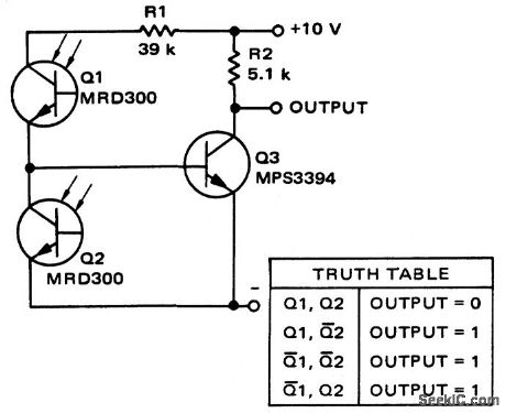
Photo-activated logic driver (courtesy Motorola Semiconductor Products Inc.). (View)
View full Circuit Diagram | Comments | Reading(664)
500_MC_SMALL_SIGNAL
Published:2009/7/10 5:45:00 Author:May
Uses 2N3570 silicon transistor to give 16 db gain.-Texas Instruments Inc., Solid-State Communications, McGraw-Hill,N.Y.,1966,p 259. (View)
View full Circuit Diagram | Comments | Reading(700)
BASIC_DARIJNGTON
Published:2009/7/10 5:44:00 Author:May
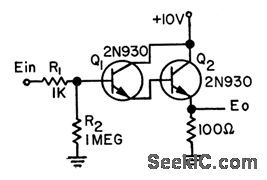
When used as betasquaring circuit, chief drawback is severe change in off'set voltage with temperctture.If base-emitter voltage varies about 2 mv per degree Q, 25℃ temperature change can give output change of 50 mv per stage.-R. C. Going, Temperature.Stabilize d Darlington, EEE, 11:7, p 28-29.
(View)
View full Circuit Diagram | Comments | Reading(649)
VIDEO_SWITCH
Published:2009/7/17 5:14:00 Author:Jessie
Used to either pass to blank out video signals going to ppi visual display. Blanking gate input pulse is applied to switch if video fails to identify itself as signal from associated radar set.-L. Turf, Video Switch for Radar, FEE, 11:2, p 24-25. (View)
View full Circuit Diagram | Comments | Reading(0)
COMPLEMENTARY_TRANSISTOR_DARLINGTON_
Published:2009/7/10 5:43:00 Author:May
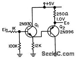
Use of complementary transistors virtually eliminates undesired offset voltages through cancelling action. Germanium transistors may be used in place of silicon units shown.-R. C, Going, Temperature-Stabilized Darlington, EEE, 11:7, p 28-29. (View)
View full Circuit Diagram | Comments | Reading(966)
Q_MULTIPLIER
Published:2009/7/10 5:43:00 Author:May
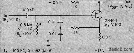
Circuit Q in single-coil arrangement is insensitive to drift in trctnsistor parameters, permitting use in filter and oscillator design.-J. R. Woodbury, Simple Transistor Q-Muhiplier or Oscillator, Electronics, 35:22, p 53-54. (View)
View full Circuit Diagram | Comments | Reading(2675)
2712_MC_RETINA_WELDER
Published:2009/7/17 5:13:00 Author:Jessie
Applies r-f energy to spot-weld retina back to original position by creating small burn scars. Crystal-controlled electron-coupled oscillator drives class C power amplifier V2. Sample of output is taken through C3, detected in V8, and applied to grid of V5, which amplifies out put changes and applies them to grid of clamp tube V3 to restore output of V2 to desired level .-O. Rick ,Jr. and R.V. Hill, R-F Spot Welder Reattaches Retina of Human Eye, Electronics, 34:32, p 160-163. (View)
View full Circuit Diagram | Comments | Reading(1465)
PREFERRED_HIGH_IEVEL_CATHODE_POLLOWER
Published:2009/7/10 5:42:00 Author:May
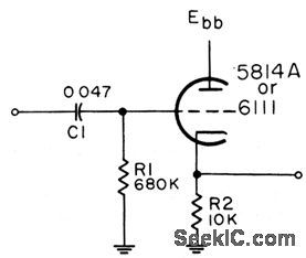
Used to isolate critical circuits from their loads, because it has high input impedance and low output impedance. Not suited for driving low-impedance transmission line, because tube would be severely overloaded.Plate voltage depends on tube used.-NBS, Handbook Preferred Circuits Navy Aero.nautical Electronic Equipment, Vol. I, Electron Tube Circuits, 1963, PC 43, p 43-2. (View)
View full Circuit Diagram | Comments | Reading(649)
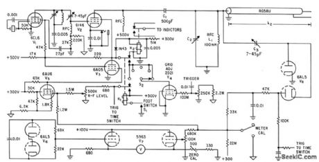
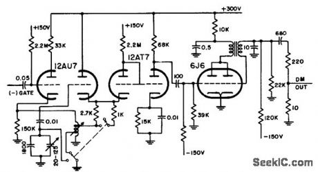
DISTANCE_MARK_GENERATOR_4
Published:2009/7/17 5:12:00 Author:Jessie
Uses switched Hartley oscillator, gated-beam amplifiershaper, and series-triggered blocking oscillator to generate distance marks for 2, 5, and and 25 miles in airborne search radar.-NBS, Handbook Preferred Circuits Navy Aeronautical Electronic Equipment, Vol. 1, electron Tube Circuits, 1963, p N8-3. (View)
View full Circuit Diagram | Comments | Reading(658)
COMPLEMENTARY_CURRENT_MULTIPLIER
Published:2009/7/10 5:41:00 Author:May
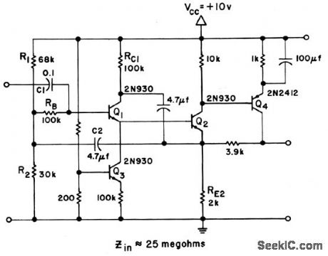
Use of complementary transistor Q4 increases current multiplicotion and increases gain at emitter of Q2 by rctising effective value of RE2. This higher gain makes bootstrapping more effective. Input impedance is 25 meg.Response is 50 cps to 1 Mc.-Texas Instruments Inc., Solid-State Communicotions, McGraw-Hill, N.Y., 1966, p 183. (View)
View full Circuit Diagram | Comments | Reading(1037)
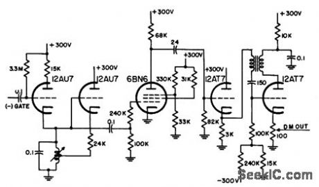
INTEGRATING_OPERATIONAL_AMPLIFIER
Published:2009/7/17 5:12:00 Author:Jessie
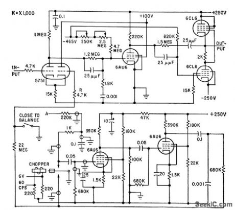
Analog-computer type of integrator uses stabilized chopper for integration of dye curve as function of time, in system for measuring dye concentration in blood stream to obtain low rate.-R. L. Skinner and D. K.Gehmlich, Analog Computer Aids Heart Ailment Diagnosis, 32:40, Electronics, p 56-59. (View)
View full Circuit Diagram | Comments | Reading(1031)
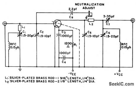
500_MC_NEUTRALIZED_AMPLIFIER
Published:2009/7/10 5:40:00 Author:May
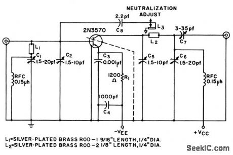
Small-signal circuit provides 17 db gain and noise figure of only 3 db. Input impedance is 51 ohms and output impedance is 1,300 ohms in parallel with 1.8 pf. Neutralizing voltage is obtained from coupling loop L3, which is silver-plated strip of beryllium copper run ning parallel to L2.-Texas Instruments Inc., Solid-State Communications, McGraw-Hill, N.Y., 1966, p 299. (View)
View full Circuit Diagram | Comments | Reading(606)
DISTANCE_MARK_GENERATOR_3
Published:2009/7/17 5:11:00 Author:Jessie
Uses switched Hartley oscillator, amplifier-shaper, and parallel-triggered blocking oscillator to generate distance marks for 10 and 40 miles in air. borne scorch radar.-NBS, Handbook Preferred Circuits Navy Aeronautical Electronic Equipment, Vol. 1, Electron Tube Circuits, 1963, p N8-3. (View)
View full Circuit Diagram | Comments | Reading(699)
TUNED_RF_WAVEMETER
Published:2009/7/10 5:40:00 Author:May
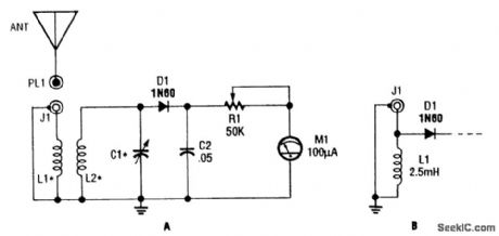
L1 and L2 form a tuned transformer. About a 1:3 turns ratio is optimum. L2 and C1 tune to the desired frequency. The frequency range can be 10 kHz to over 200 MHz, depending on the value of C1.For HP use, C1 can be a 140-pF variable. For VHF, use about 25 μF. Use of a 2.5 pH RE choke will yield an untuned wavemeter. (View)
View full Circuit Diagram | Comments | Reading(886)
| Pages:812/2234 At 20801802803804805806807808809810811812813814815816817818819820Under 20 |
Circuit Categories
power supply circuit
Amplifier Circuit
Basic Circuit
LED and Light Circuit
Sensor Circuit
Signal Processing
Electrical Equipment Circuit
Control Circuit
Remote Control Circuit
A/D-D/A Converter Circuit
Audio Circuit
Measuring and Test Circuit
Communication Circuit
Computer-Related Circuit
555 Circuit
Automotive Circuit
Repairing Circuit