
Circuit Diagram
Index 813
RC_COUPLED_FET_AMPLIFIER
Published:2009/7/10 5:39:00 Author:May
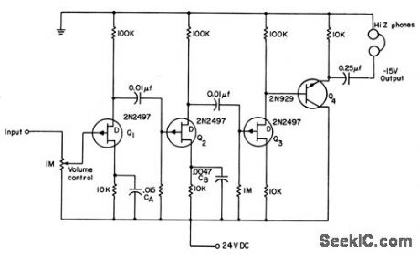
Used fo drive high-impedcmce headphones in optical com muniation system. Series peaking capacitors CA and CB compensate for high-frequemcy inadequacies in rest of system. No Ictrge electrolytics are needed. Without pecking cctpacitors, amplifier vohage gain is about 400 and upper amd lower break frequendes are 17 cps and 35 kc.-L. J. Sevin, Jr., Field-Effect Transistors, McGraw-Hill, N.Y, 1965, p 64. (View)
View full Circuit Diagram | Comments | Reading(849)
PULSE_WIDTH_DISCRIMINATOR
Published:2009/7/17 5:09:00 Author:Jessie
Cuts scanning loss from interfering radars in half, by blanking video signal only if it falls within notch developed by gating circuits. Gives marked improvement in acquisition capability.-K. H. Chase and J. L. Pierzga, Reducing Mutual Radar Interference, Electronics, 32:28, p 39-43. (View)
View full Circuit Diagram | Comments | Reading(1931)
LOW_SOURCE_IMPEDANCE
Published:2009/7/10 5:38:00 Author:May
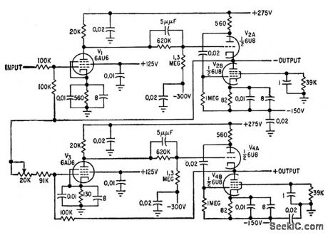
Tubes V1 and V2 provide single-phase inversion with output impedance below 0.5 ohm over 50.kc poss bond when feedback loop is dosed. Output of V2 feeds identical combination V3-V4 to provide second output in phase with input to V1. Trim adjustment is provided to insure unity gain for both outputs. Used in automatk doppler cycle counter for measuring position and velocity of missiles.-B. E. Keiser, Digital-Countor Techniques Increase Doppler Uses, Electronics, 32:21, p 46-50. (View)
View full Circuit Diagram | Comments | Reading(666)
PRECISION_CRYSTAL_FREQUENCY_CHECHER
Published:2009/7/10 5:38:00 Author:May
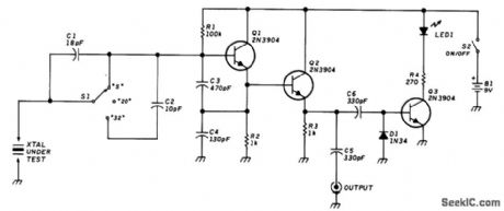
This circuit uses a Colpitts oscillator (Q1) with a buffer amplifier (Q2) to test crystals. S1 selects three load conditions-series (S), 20 pF, and 32 pF. Leads to S1 and the crystal should be kept short. The circuit should be useful over 2-to 20-MHz. (View)
View full Circuit Diagram | Comments | Reading(724)
OUT_OF_BASEBAND_NOISE_AMPLIFIER
Published:2009/7/17 5:09:00 Author:Jessie
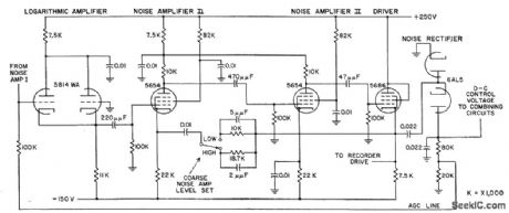
Provides transfer function that is essentially logarithmic, with slop of 5 to 7 db per octave, to serve as bias volage for differentical combiner of i-f amplifier in troposcatter f-m receiver. Amplifier control range extends 40 db above threshold. Signal-noise ratio of highest baseband channel is 70 db.-P. Gruber, Crystal Converter for Tropo-Scatter Receivers, Electronics, 31:15, p 78-82. (View)
View full Circuit Diagram | Comments | Reading(1034)
455_kHz_AM_IF_SIGNAL_GENERATOR
Published:2009/7/10 5:36:00 Author:May
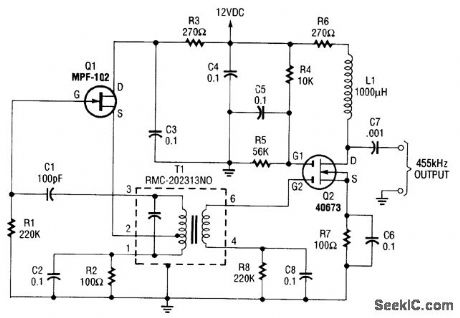
An MPF102 FET oscillator drives a dual-gate MOSFET buffer.The MPF102is configured as aHartley oscillator.If desired,an audio voltage can be coupled to the junction of R4,R5,and CS with anextra coupling capacitor(≈1μF) to AM modulate the signal.T1=Toko P/N RMC-202313NO. (View)
View full Circuit Diagram | Comments | Reading(2833)
DISTANCE_MARK_GENERATOR_2
Published:2009/7/17 5:07:00 Author:Jessie

Uses switched Hartley oscillator, pentode amplifier-shaper, and series-triggered blocking oscillator to generate 1-mile distance marks in airborne search radar. Frequency dividers are used for 10- and 20-mile marks.-NBS, Handbook Preferred Circuits Navy Aeronautical Electronic Equipment, Vol. 1, Electron Tube Circuits, 1963, p N8-2. (View)
View full Circuit Diagram | Comments | Reading(768)
LOW_LEVEL_1_CPS_TO_500_KC
Published:2009/7/10 5:35:00 Author:May
Features indude input impedance above 30 meg and noise figure below 3 db over wide range of generator resistantes. Bootstrapping of input stage enhances high input impedance of fet. Will operate down to 1 cps without need for large capacitors. Upper frequency limit is 500 kc for generator resistance of 100K. Voltage gain is stable within 0.5 db of 40, from -55 to +125℃.-Texas Instruments Inc., Solid-State Qommunicotions, McGraw.Hill, N.Y., 1966, p 290. (View)
View full Circuit Diagram | Comments | Reading(722)
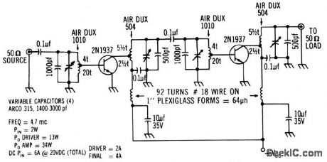
HIGH_VOLTAGE_GAIN
Published:2009/7/10 5:33:00 Author:May
Provides gain of 3,500 into 10-meg load, by operating transistor in common-base configuration and using constant-current source in collector drcuit, Circuit is balanced, so either transistor can operctie as gain stage while other serves as current source. Feedback overcomes problem of critial d-c bias.-A. J. Adler, High-Gain Ampliner, EEE, 11:8, p 31. (View)
View full Circuit Diagram | Comments | Reading(706)
CASCADED_EMITTER_FOLLOWER_WITH_CURRENT_BIAS
Published:2009/7/10 5:33:00 Author:May
Improved frequency response is obtained by biasing Q1 with current generator in emitter or leg.Input impedance is 6 meg. Frequency response is within 3 db from 10 cps to 1 Mc,-Texas Instruments Inc., solid-Stale Communications, McGraw-Hill.N.Y., 1966,p 181. (View)
View full Circuit Diagram | Comments | Reading(853)
SINGLE_OPAMP_
Published:2009/7/10 5:33:00 Author:May
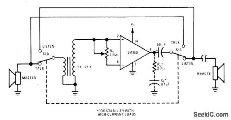
When switch S1 is in talk position as shown, loudspeaker of master station acts as microphone, driving opamp through step-up transformer T1. Switch at remote station must then be in listen position. Supply voltage range is 8-20 V.- Audio Handbook, National Semiconductor, Santa Clara, CA, 1977, p 4-21-4-28. (View)
View full Circuit Diagram | Comments | Reading(810)
Frequency_sensitive_photo_activated_alarm
Published:2009/7/17 5:07:00 Author:Jessie
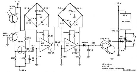
Frequency-sensitive photo-activated alarm (courtesy Motorola Semiconductor Products Inc.). (View)
View full Circuit Diagram | Comments | Reading(934)
FREQUENCY_COUNTER
Published:2009/7/10 5:32:00 Author:May
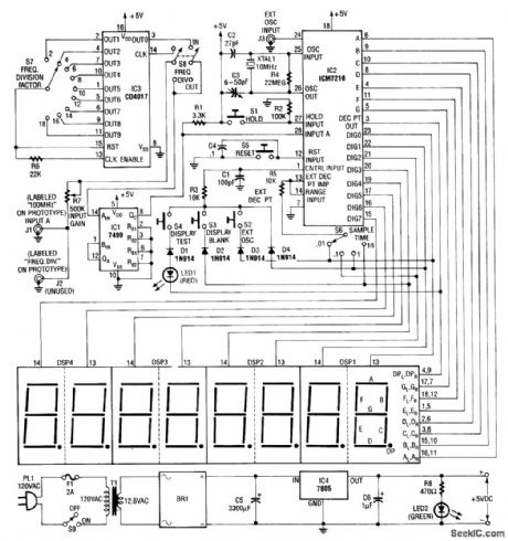
Built around an Intersil 7216 frequency-counter IC, this counter has a basic range of 10 MHz, a 100-MHz prescaler, and an extra frequency divider (IC3). This divider divides 'oy an extra factor, as marked on S7 (see schematic), to extend the range of the counten The display is multiplexed. MAN6710 2-digit red common anode 7-segment LED displays were used on the prototype. (View)
View full Circuit Diagram | Comments | Reading(0)
47_MC_DRIVER_AND_AMPLIFIER
Published:2009/7/10 5:32:00 Author:May
Common-emiller connection gives good power gain with collector-emitter voltage of 20 v,though gain varies with frequency.-Texas Instruments Inc., Solid.State Communications, McGraw-Hill, N.Y., 1966, p 316. (View)
View full Circuit Diagram | Comments | Reading(787)
12_V_AT_2_A
Published:2009/7/17 5:06:00 Author:Jessie
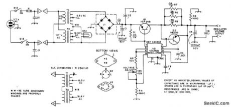
Will operate 10-W 220-MHz portable FM transceiver from AC line. Output voltage is adjustable from 9 to 13 V. DC voltage at point A is about 30V. U1 is 50-V 10-A bridge rectifier Ripple voltage on output is less than 30 mV P-P. - E. Kalin, A No-Junkbox Regulated Power Supply, QST, Jan. 1975, p 30-33. (View)
View full Circuit Diagram | Comments | Reading(1020)
±5_TO_±18V_WITH_TRACKING
Published:2009/7/17 5:05:00 Author:Jessie
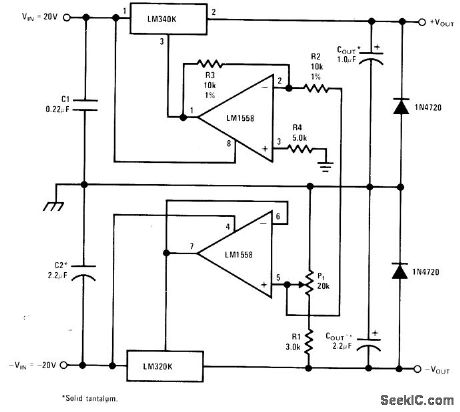
Ground pin of LM1558 inverter, while ground pin of negative LM320K-15 is lifted by LM1558 voltage follower. Positive regulator is madeto track negative regulator within about 50 mV over entire output range. At ±15V, typical load regulation is between 40 and 80 mV for 0-1 A pulsed load.- Linear Applications, Vol. 2, National Semiconductor, Santa Clara, CA, 1976, AN-103, p 8-9. (View)
View full Circuit Diagram | Comments | Reading(976)
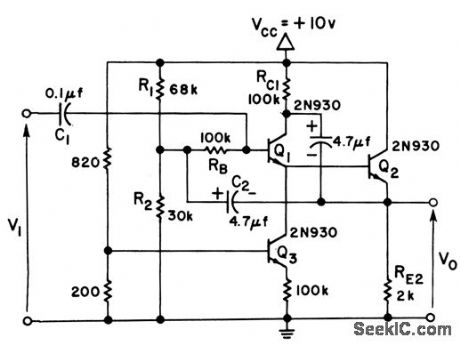
SIGNAL_VOLTAGE_STABILIZER
Published:2009/7/10 5:31:00 Author:May
Main amplifier is followed by emffier-followers to reduce fraction of d-c load current fowing in collector load of omplifier. In this conventional arrangement, overall gain is only about 500.-T. K. Hemingway, Applications of the Constant-Current Diode, Electronics, 34:42, p 60-63. (View)
View full Circuit Diagram | Comments | Reading(547)
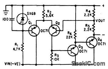
DETECTION_IN_NOISE
Published:2009/7/17 5:05:00 Author:Jessie
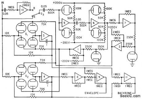
Time derivatives of noise-contaminated input signals control electronic switches which control sampling and holding unit. In mode for detection, signal is sampled at its peaks and troughs. In mode for backbone detection, involving additive noise, signal is sampled at its inflection points.-N. D. Diamantides, Nonlinear Filter Detects Envelope or Backbone, Electronics, 35:18, p 52-54. (View)
View full Circuit Diagram | Comments | Reading(1023)
EMITTER_FOLLOWER_LED_DRIVER
Published:2009/7/10 5:30:00 Author:May
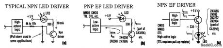
Using emitter/followers saves parts and simpliftes LED driver loading on logic circuitry. (View)
View full Circuit Diagram | Comments | Reading(1011)
FOUR_STATION_TWO_WAY
Published:2009/7/10 5:30:00 Author:May
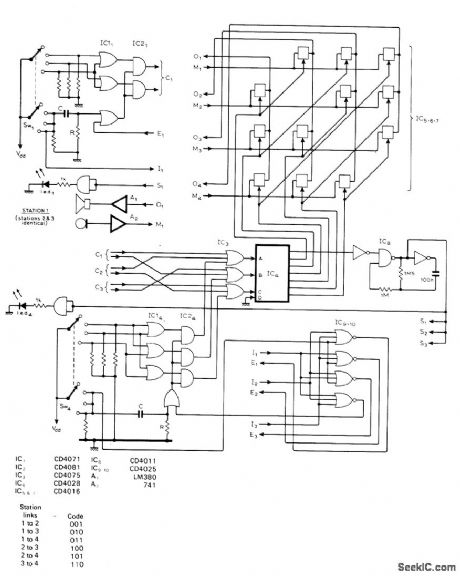
Each station can commumcate pnvately with any one of others.All four stations have identical inputs as at upper left, with fourth station having master circuit. Each two-station combination is assigned 3-bit code as given in table, for selection by switches Sw1-Sw4 All station codes are ORed and decoded by IC4 to drive matrix of analog switches for coupling appropriate audio inputs and outputs. Code 000 is used for systemfree status as indicated by LEDs 1 and 4 being on. LEDs flash for system-busy status. When code is selected, enable inputs of nonselected stations go low to prevent generation of further codes. System can be expanded to six stations by using 4-bit code and CD4514 decoder with larger matrix of analog switches.-B. Voynovich, Multiple Station Two-Way Intercom, Wireless World, March 1978, p 59. (View)
View full Circuit Diagram | Comments | Reading(939)
| Pages:813/2234 At 20801802803804805806807808809810811812813814815816817818819820Under 20 |
Circuit Categories
power supply circuit
Amplifier Circuit
Basic Circuit
LED and Light Circuit
Sensor Circuit
Signal Processing
Electrical Equipment Circuit
Control Circuit
Remote Control Circuit
A/D-D/A Converter Circuit
Audio Circuit
Measuring and Test Circuit
Communication Circuit
Computer-Related Circuit
555 Circuit
Automotive Circuit
Repairing Circuit