
Circuit Diagram
Index 819
STABILIZING_GAIN
Published:2009/7/10 4:55:00 Author:May
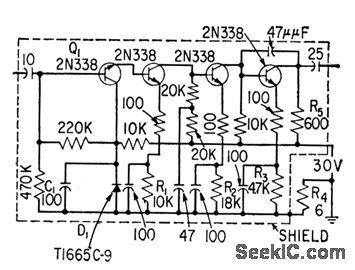
Use of negative feedback in four-stage direct-coupled amplifier keeps gain constant within 1 db of 40 db from 6 cps to 300 kc. Input impedance is 8 meg end output impedance is 600 ohms.-Feed-back Increases Input Impedance, Electronics, 32:11, p 150-153. (View)
View full Circuit Diagram | Comments | Reading(581)
10_position_SCR_crowbar_life_test_fixture
Published:2009/7/19 20:37:00 Author:Jessie
10-position SCR crowbar life test fixture (courtesy Motorola Semiconductor Products Inc.). (View)
View full Circuit Diagram | Comments | Reading(1111)
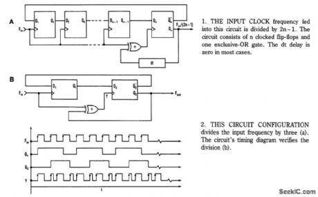
DIVIDE_BY_ODD_NUMBER_COUNTER
Published:2009/7/10 4:55:00 Author:May
This circuit symmetrically divides an input by virtually any odd number. The circuit contains n+l/2 clocks twice to achieve the desired divisor. By selecting the proper n, which is the decoded output of the 74LS161 counter, you can obtain diisors from 3 to 31. This circuit divides by 25; you can obtain higher divisors by cascading additional LS161 counters.
The counter and IC5A form the n+l/2 counter. Once the counter reaches the decoded counts, n, IC5A ticks off an additional 1/2 clock, which clears the counter and puts it in hold. Additionally, IC5A clocks IC5B, which changes the dock phasing through the X0R gate, IC1. The next edge of the input clocks IC5A, which reenables the counter to start counting for an additional n+l/2 cycles.
Although the circuit has been tested at 16 MHz, a worst-case timing analysis reveals that the maxi-mum input frequency is between 7 and 8 MHz. (View)
View full Circuit Diagram | Comments | Reading(2523)
TTL_SOA_test_circuit
Published:2009/7/19 20:35:00 Author:Jessie
TTL SOA (safe operating area) test circuit (courtesy Motorola Semiconductor Products Inc.). (View)
View full Circuit Diagram | Comments | Reading(910)
2_W_WITH_IC
Published:2009/7/10 4:54:00 Author:May
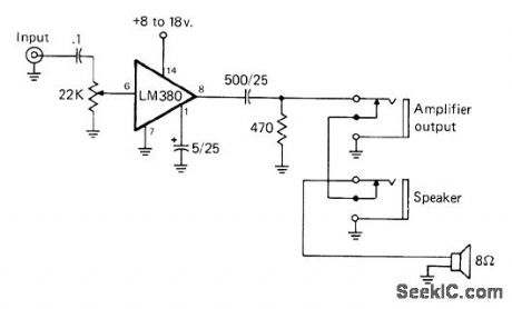
lnexpensive audio amplifier using 14-pin DIP provides adequate power for small audio projects and audio troubleshooting.Pins 3, 4, 5, 10, 11, and 12 are soldered directly to foil side of printed-wiring board used for construction,to give effect of heatsink.-J. Schultz, An Audio Circuit Breadboarder's Delight, CQ, Jan. 1978, p 42 and 75. (View)
View full Circuit Diagram | Comments | Reading(1531)
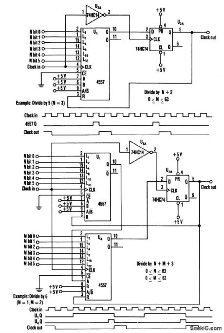
PROGRAMMABLE_FREQUENCY_DIVIDER
Published:2009/7/10 4:54:00 Author:May
This divider uses a variable-length shift register, a type-D flip-flop, and an inverter. The clock feeds the flip-flop clock input and the output of the shift register feeds the D input of the flip-flop. The FF output is tied back to the reset input of the shift register so that each clock pulse shifts a 1 into the 4557. N+ 1 cycles after the reset pulse is removed. The first 1 will propagate through the register output. The 1 is latched into the FF on the clock's next falling edge and fed back to the 4557 reset pin, which resets the shift register to zero. When a zero is clocked into the flip-flop on the next falling clock edge, the reset is removed, restarting the process. The divide ratio is (N+2), where N = the binary number that is programmed into 4557. (View)
View full Circuit Diagram | Comments | Reading(1608)
ELECTRONIC_ANTENNA_SELECTOR
Published:2009/7/10 4:54:00 Author:May
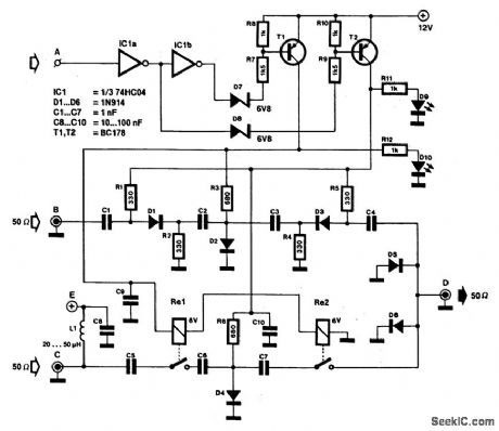
The electronic antenna selector is intended to switch between two FM antennas via a logic signal. Gates IC1A and IC1B ensure a clean switching action and at the same time form the interface between the 5-V logic level (probably available from the receive) and the 12-V supply voltage for the selecton Depending on the type of gate used, a digital TTL or CMOS control signal is available in direct and inverted form at the outputs of IC1.When input A is logic high, the output of IC1A is low and that of IC1B is high. The current then flows from the positive supply line to IC1A via T2, R9, and D8. T2 is switched on and D9 lights.Because direct currents flow through R1/D1/R2 and R5/D3/R4, diodes D1 and D3 conduct and pass the VHF signal from input A to output D. At the same time, a direct current flows through R6/D4 so that D4 conducts. This arrangement ensures that any VHF signal at input C cannot reach the output via the parasitic capacitances of the relay contacts and the wiring.When A is logic low, and IC1B is therefore low, the current flows from the positive supply line to IC1B via T1, R7, and D17. T1 is then switched on and D10 lights. At the same time, the two series-connected relays, Re1 and Re2, are energized, their contacts close, and the VHF signal at input C is fed to output D. Moreover, a direct current flows through R3/D2 so that D2 conducts. Any signal at input B is then shorted to ground via D2.All resistors should be carbon-film types because these have a higher parasitic series inductance than metal-film resistors. Thus, the attenuation of the VHF signal caused by them is reduced to a minimum.The attenuation losses caused by the diode junctions (5-10 dB) are somewhat larger than those caused by the relays. It is thus advisable to connect the antenna that provides the weaker signal (normally the domestic one) to input C. If the domestic antenna is equipped with an antenna amplifier, it can be supplied via terminal E. Diodes D5 and D6 protect the circuit against high-voltage spikes that occur during the on and off switching. The selector draws a current of approximately 65 mA. (View)
View full Circuit Diagram | Comments | Reading(847)
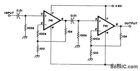
CASCADED_741_OPAMPS
Published:2009/7/10 4:51:00 Author:May

Two opamps in series provide 80 dB of audio gain with bandwidth of about 300 to 6000 Hz. Gain of each opamp is set at 100. With three stages, bandwidth would be 5100 Hz. Output will drive loudspeaker at comfortable room level, if fed through 1-μF nonpolarized capacitor to output transformer having 500-ohm primaryand 8-ohm secondary.-C.Hall, Circuit Design with the 741 Op Amp, Ham Radio, April 1976, p 26-29. (View)
View full Circuit Diagram | Comments | Reading(1040)
Oscilloscope_calibrator_using_an_LM3909_chip
Published:2009/7/19 20:25:00 Author:Jessie
Oscilloscope calibrator using an LM3909 chip. The output is a clean rectangular wave that is exactly 1 volt peak to peak. The rectangular wave is approximately 1.5 ms on and 5.5 ms off. Battery life from a 1.5-volt D-cell is approximately 500 hours (courtesy National Semiconductor Corporation). (View)
View full Circuit Diagram | Comments | Reading(716)
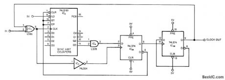
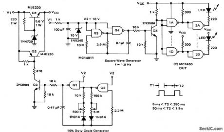
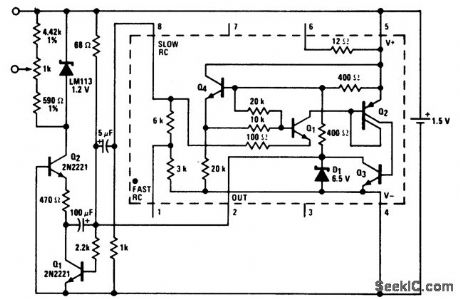
CLOCK_INPUT_FREQUENCY_DIVIDER
Published:2009/7/10 4:50:00 Author:May

ICA, R1 through R3, and Q1 form a current source. The current that charges C1 is given by:
The input signal drives ICD. Because ICD's positive input (V+) is slightly offset to +0.1 V, its steady-state output will be near + 13 V. This voltage is sent to ICC through D2, setting ICC's output to +13 V. Therefore, point D is cut off by D1, and C1 is charged by the current source. Assuming the initial voltage on C1 is zero, the maximum voltage (I/Cmax) is given by:
The right side of the inequality should be the minimum pulse width (either up time or down time) of the input clock. The circuit, when constructed with standard 74F-type parts, operates without any added delay in the exclusive-0R feedback path and with an input frequency of up to 22.5 MHz. The circuit's output signal will have the same duty cycle as the input clock. (View)
View full Circuit Diagram | Comments | Reading(1132)
CONTINUITY_TESTER_1
Published:2009/7/10 4:49:00 Author:May
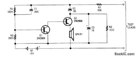
A continuity tester that has an audible indicator can be more useful in some cases than a visual indicator, because you need not take your eyes from the job at hand. Q1 and Q2 form an audio oscillator. When the test leads are connected to a continuous circuit, the oscillator operates, and sounds a tone from the speaker. (View)
View full Circuit Diagram | Comments | Reading(1889)
MICROPOWER_ONE_WAY_INTERCOM_
Published:2009/7/10 4:47:00 Author:May
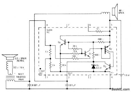
National LM3909 IC operating from single 1.5-V cell serves as low-power one-way intercom suitable for listening-in on child's room and meeting other room-to-room communication needs. Battery drain is only about 15 mA. Person speaking directly into 3.2-ohm loudspeaker used as microphone delivers full 1.4 V P-P signal to 40-ohm loudspeaker at listening location.- Linear Applications, Vol. 2, National Semiconductor, Santa Clara, CA, 1976, AN-154, p 9. (View)
View full Circuit Diagram | Comments | Reading(1109)
Buzz_box_continuity_and_coil_checker_using_an_LM3909_chip
Published:2009/7/19 20:24:00 Author:Jessie
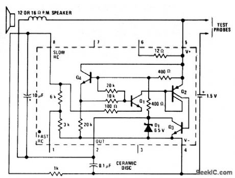
Buzz box continuity and coil checker using an LM3909 chip. Circuitry inside dashes is the LM3909. A short up to 100 ohms will cause a tone to be generated. By probing two values, such as a direct short and 5 ohms, a difference can be detected if done in quick succession (courtesy National Semiconductor Corporation). (View)
View full Circuit Diagram | Comments | Reading(834)
RADIO_DIRECTION_FINDER_
Published:2009/7/10 4:46:00 Author:May
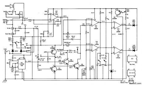
This RDF circuit consists of a square-wave oscillator (IC1), which switches two antennas alternately at an audio rate. A phase detector (Q1, 2, 3, 7) is used to compare receiver output amplified by IC2 with the reference phase from IC2 with the reference phase from IC1. A 50-μA meter is used as a left-right indicator. IC3 is a comparator used to drive indicator LEDs. (View)
View full Circuit Diagram | Comments | Reading(2360)
DC_meter_protection_circui
Published:2009/7/19 20:23:00 Author:Jessie
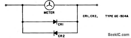
DC meter protection circuit. The diodes will not conduct until the voltage across the meter reaches 0.5 to 0.7 volts. For a typical meter movement with an internal resistance of 1200 ohms and a full-scale current rating of 50 μA the rectifiers will introduce less than 1% error (courtesy General Electric Company). (View)
View full Circuit Diagram | Comments | Reading(914)
Watt_hour_meter
Published:2009/7/19 20:23:00 Author:Jessie
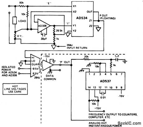
Watt-hour meter. The output of the 284J represents the instantaneous power delivered to the load, which is a 40-watt light bulb. This signal is averaged and converted to a frequency by the AD537 V/F converter. The pulse repetition rate of be AD537 varies in direct proportion to the average power consumed by the 40-watt light bulb. Different sensitivities (e.g., watt-minutes, watt-seconds, etc.) can be obtained by altering the scale factor of the AD537, the gain of the 284J or the count ratio on the AD537 output. lf an analog output is desired, an analog integrator can be successfully employed within the limitations shown (courtesy Analog Devices, Inc.). (View)
View full Circuit Diagram | Comments | Reading(1937)
dc_MILLIVOLTMETER
Published:2009/7/10 4:44:00 Author:May
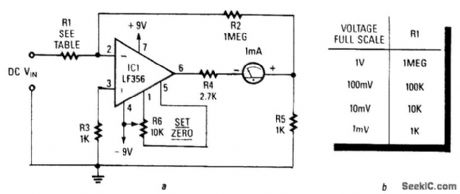
An LF356 op amp is used as a gain amplifter with the output taken across R5. When a full-scale current of 1 mA is flowing through the meter, exactly 1V appears across R5 (should be 1% tolerance or better). This is fed back to R2 to the summing junction of IC1 (a full-scale produces 1μA). This offsets the current through R1. R1 has a value of 1 MΩ/V which is used to zero the meter. R4 provides some overcur-rent protection for the meter. (View)
View full Circuit Diagram | Comments | Reading(2384)
Sample_and_hold_circuit_with_Av_=_1___RF_RL
Published:2009/7/19 20:21:00 Author:Jessie
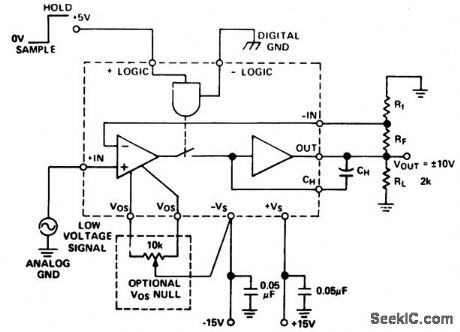
Sample-and-hold circuit with Av = (1 + RF/RL). Circuitry inside dashed lines is the AD582 sample-and-hold amplifier (courtesy Analog Devices, Inc.). (View)
View full Circuit Diagram | Comments | Reading(1510)
High_speed_sample_and_hold_circuit_using_an_ECG915_operational_amplifier
Published:2009/7/19 20:20:00 Author:Jessie
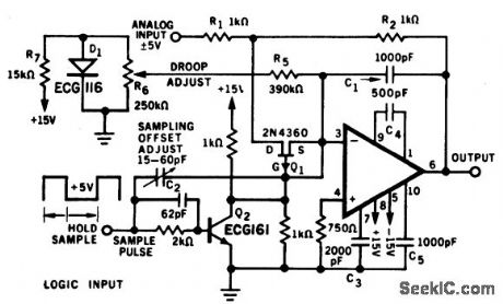
High-speed sample-and-hold circuit using an ECG915 operational amplifier (courtesy GTE Sylvania Incorporated). (View)
View full Circuit Diagram | Comments | Reading(672)
Noninverting_unity_gain_sample_and_hold_circuit_using_a_Datel_SHM_IC_1
Published:2009/7/19 20:19:00 Author:Jessie
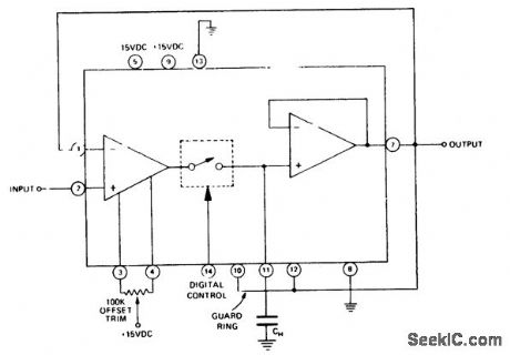
Noninverting unity-gain sample-and-hold circuit using a Datel SHM-IC-1. The SHM-IC-1 is a 14-pin DIP with a 2 MHz bandwidth. The 100 K offset pot should be a 100 PPM/℃ 15-turn type, available from Datel. To zero ground pin 2 and pin 14, then adjust offset for zero output at pin 7 (courtesy Datel Systems, Inc.). (View)
View full Circuit Diagram | Comments | Reading(885)
| Pages:819/2234 At 20801802803804805806807808809810811812813814815816817818819820Under 20 |
Circuit Categories
power supply circuit
Amplifier Circuit
Basic Circuit
LED and Light Circuit
Sensor Circuit
Signal Processing
Electrical Equipment Circuit
Control Circuit
Remote Control Circuit
A/D-D/A Converter Circuit
Audio Circuit
Measuring and Test Circuit
Communication Circuit
Computer-Related Circuit
555 Circuit
Automotive Circuit
Repairing Circuit