
Circuit Diagram
Index 802
AUXILIARY_SUPPLY
Published:2009/7/10 21:54:00 Author:May
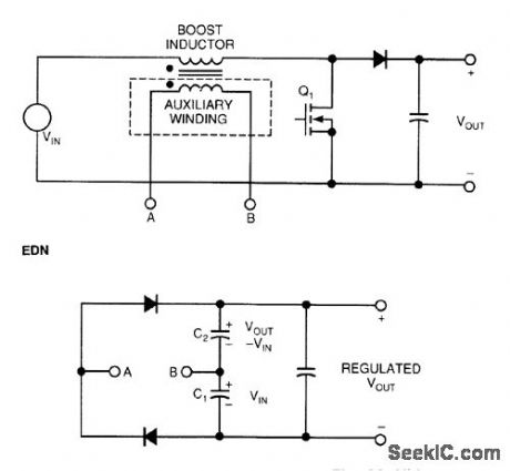
Many power-factor-correction circuits use a boost converter to generate a regulated dc output voltage from the ac line input while forcing the load to draw sinusoidal current, which maximizes the power factor.
This circuit's full-wave rectifter the auxiliary winding's output to completely cancel out line variations and provide a regulated output voltage. The circuit essentially sums the two phases of the boost inductor's voltage to eliminate the 120-Hz components. The regulated output tracks the power-factor-controlled pre-regulator output voldage and it can be used in the corrected output voltage's feedback loop.
An isolated auxiliary winding consists of the desired number of turns wound on the boost inductor. You can vary the exact value of the auxiliary supply's output voltage by adjusting or scaling the auxiliary wind-ing's number of tums. Figure 63-4(b)'s rectifter develops two separate, but individually unregulated volt-ages, across capacitors C1 and C2. Each of these voltages varies in amplitude at twice the ac-line frequency. When switch Q1 is on, the boost inductor connects directly across the input supply, and a volt-age proportional to the instantaneous input voltage develops across capacitor C1.
Once the switch tums off, the inductor voltage reverses and clamps to a voltage equal to VOUT -VIN. During this interval, a voltage proportional to VOUT -VIN develops across C2. The sum of these two capac-itor voltages produces a regulated auxiliary voltage that is proportional to VOUT. The voltage across the output capacitor equals VIN+ (VOUT- VIN), which cancels the input-line variations. (View)
View full Circuit Diagram | Comments | Reading(1037)
Norton_AND_gate_and_NAND_gate_with_high_fan_out
Published:2009/7/17 4:38:00 Author:Jessie
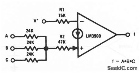
This circuit uses one section of an LM3900 to form a three-input AND gate with a fan out of 50. One of the 24-kΩ resistors and R2 can be omitted to form a two-input AND gate. Interchange the inputs to form a NAND gate. National semiconductor, Linear Applications Handbook 1991 p 240. (View)
View full Circuit Diagram | Comments | Reading(723)
400_CPS_MECHANICAL_CHOPPER_AMPLIFIER
Published:2009/7/10 21:53:00 Author:May
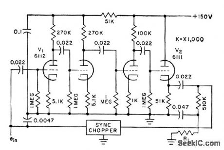
Chopper modulates incoming d-c signal for a-c amplification, then demodulates output synchronously. Conversion gcdn is above 5,000. Suitable for high-goin low-level strcdn.gage thermocouple, and similar signcds where amplifier drift must be minimized without us ing regulated power supply.-L.S. Klivans, D-C Amplifiers for Control Systems, Electronics, 31:47, p96-100. (View)
View full Circuit Diagram | Comments | Reading(784)
UNIVERSAL_SUPPLY
Published:2009/7/17 4:38:00 Author:Jessie
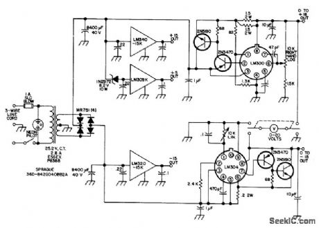
Provides three different fixed voltages and two variable, each regulated and each current-limited at 1.5 A for use on experimenter's bench. Use heatsinks for fixed voltage regulators and for output transistors. - N. Calvin, Universal Power Supply, 73 Magazine, Aug. 1974, p 65-66. (View)
View full Circuit Diagram | Comments | Reading(857)
DYNAMIC_FOCUS_CORRECTION
Published:2009/7/10 21:53:00 Author:May
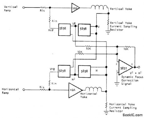
Provides sum of squares of vertical and horizontal position voltages, as required for focus correction in high-resolution flat-face magnetically deflected CRT. Circuit uses Optical Electronics 5898 fourquadrant analog multipliers to give required squared outputs, along with 9831 opamp having comparable bandwidth. Input summing resistors forhorizontal and vertical, deflection am plifiers are chosen for compatibilitj with amplifiers being used. Select current-sampling resistors to generate 10-V peak signaL- Dynamic Focus Correction with Analog Function Modules, Optical Electronics, Tucson, AZ, Application Tip 10127. (View)
View full Circuit Diagram | Comments | Reading(753)
CAVE_MAPPING_TRANSMITTER
Published:2009/7/17 4:37:00 Author:Jessie
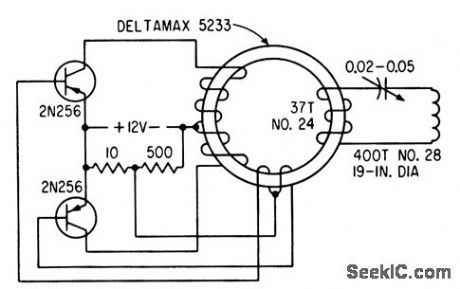
Transistorized 5-w, 2,000-cps generator of low-frequency magnetic induction fold direction finder feeds tuned loop in cave being mapped. Detector at surface locates vertical flux line over cave and also receives Morse code for communication.-E. R. Roesehlein, Mapping Caves Magnetically, Electronics, 33:39, p 61. (View)
View full Circuit Diagram | Comments | Reading(2757)
TRACE_QUADRUPLER
Published:2009/7/10 21:52:00 Author:May
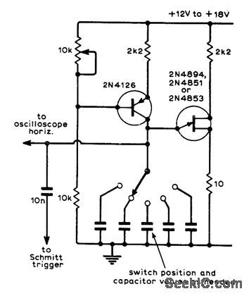
Designed for use with DC oscilloscopes. Constant-current UJT oscillator produces linear sawtooth for triggering Schmitt trigger and serving as hodzontal sweep voltage. Frequency is varied by switching capacitors, and can be up to about 100 kHz. Emitter-follower may have to be added to UJT output to prevent loading of timing capacitors by low impedance of Schmitt trigger. Used to quadruple maximum time-base frequency of oscilloscope.-J. A Titus. Trace Quadrupler, Wireless World, Oct. 1972, p 479. (View)
View full Circuit Diagram | Comments | Reading(939)
OUTPUT_STABILIZER
Published:2009/7/10 21:51:00 Author:May
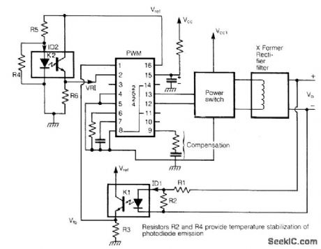
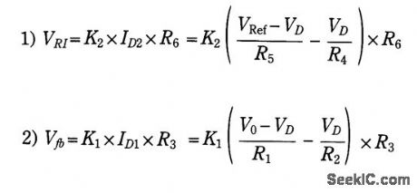

Optically isolated SMPS and dc-to-dc converters face the variance of output voltage owing to the change of transmission characteristics of an optoisolator with (a) temperature and (b) aging. The photo diode emission decays with temperature and time, and causes the output voltage to change. The problem is solved using a homoeopathic principle. An additional optical isolator is used to derive the +Ve input volt-age, instead of a conventional potential divider from internally stabilized reference. A scheme is shown using IC2524 as PWM element:where VD=forward drop of a photo diode. In equations 1 and 2, the terms:decrease with temperature. Thanks to -Ve, temperature coefficient of VD any changes in K1, and K2, as a result of temperature and aging, track each other to maintain the output voltage constant. With proper selection of R2 and R, the output voltages are found to vary by less than 0.01%/℃ over a wide tempera-ture range. (View)
View full Circuit Diagram | Comments | Reading(683)
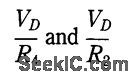
LANGMUIR_ELECTRON_DENSITY_PROBE
Published:2009/7/17 4:36:00 Author:Jessie
Used in Aerobee sounding rocket to measure day time sporadic-E ionization of upper atmosphere. Electrometer uses 100% feedback and Thyrite resistor to produce compressed scale on telemetry record.-M. F. Wolff, Rockets Probe Sporadic-E, Electronics, 35:211, p 18-19. (View)
View full Circuit Diagram | Comments | Reading(755)
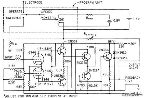
YAMPLIFIER_WITH_10_MHz_BANDWIDTH
Published:2009/7/10 21:51:00 Author:May
Rise time is 40 ns. Tr1-Tr4 form constant-current tail, with Tr5 improving linearity. Tr6 and Tr7 are complementary emitter-followers, as also are Tr8 and Tr9, for feeding deflection plates. Input should be from 50-ohm source to achieve full bandwidth. Other complementary small-signal transistors rated above 200 V can be used.-B.J. Frost, Wideband Y Amplifier for Oscilloscope, Wireless World, June 1976, p 71. (View)
View full Circuit Diagram | Comments | Reading(929)
REMOITE_CONTROLLED_TELEPHONE_FAX_MACHINE_SWITCH
Published:2009/7/10 21:50:00 Author:May
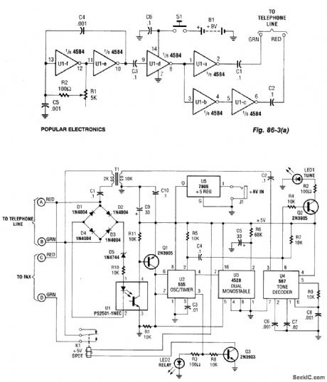
This system uses a transmitter at around 100 kHz (see Fig. 86-3(a)) to control a remote receiver. A line splitter can be used to connect the transmitter to the telephone line in use. The transmitter is a CMOS oscillator and has output buffer stages to drive the telephone line.When the receiver (Fig. 86-3(b)) detects the off-hook condition (the line voltage drops from about 48 V to less than 10 V). Optocoupler U1 has the LED extinguished. This enables timer U2. When the transmitter is activated, tone decoder U4 detects the 100-kHz signal and outputs a low signal, which lights indicator LED1. LED1 is also used to set the transmitter frequency. Also, U2 is triggered. U2 is configured for the latching condition. U2 feeds the base of Q3, turns it on and energizes relay K1, which switches in the fax machine to the telephone line.U3 prevents U2 from being accidentally triggered by transients on the telephone line. When the phone is lifted off-hook and it resets U2 after about one or two seconds of delay, transients are allowed to subside before U2 is reset, and it waits for a negative pulse on pin 2 to turn on. When U2 turns on, Q3 is biased on, which activates change-over relay K1. (View)
View full Circuit Diagram | Comments | Reading(1236)
Norton_OR_gate_and_NOR_gate_with_high_fan_out
Published:2009/7/17 4:36:00 Author:Jessie
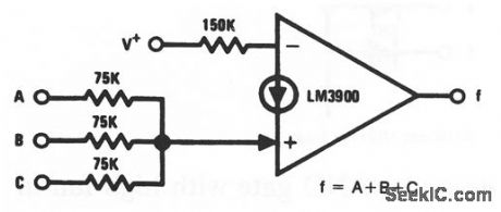
This circuit uses one section of an LM3900 to form an OR gate with a fan out of 50 gates (if each gate has a 75-kΩ input resistor). More than three inputs can be OR' ed if desired. The circuit can be converted to a NOR gate when the inputs are interchanged. National Semiconductor Linear Applications Handbook 1991, p 240 (View)
View full Circuit Diagram | Comments | Reading(693)
PENTODE_CHOPPER
Published:2009/7/10 21:50:00 Author:May
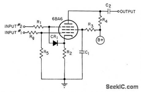
Designed for use as first stage of wide-band amplifier(d-c up to several kc).Design procedure is given.For 150V plate supply,typical values are R2=100ohms.R4=5K,R3=110K,R1=15K with 1N34A diode,R5=1meg,Rg=1K,and C1 depends on lowest frequency to be amplified.-D.G.Knox,Electronic Chopper,EEE,10:11,p 27-28. (View)
View full Circuit Diagram | Comments | Reading(726)
Norton_phase_locked_loop
Published:2009/7/17 4:36:00 Author:Jessie
This circuit uses three sections of an LM3900 to form a phase-locked loop (with a center frequency of about 3 kHz using the values shown). National Semiconductor Linear Applications Handbook 1991 p 239 (View)
View full Circuit Diagram | Comments | Reading(957)
SCOPE_PREAMP
Published:2009/7/10 21:45:00 Author:May
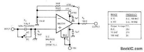
Extends vertical sensitivity range of scope or VOM at minimum cost. Voltage at output is in phase with input. Switch across C gives choice of AC or DC operation.Table gives frequency and output voltage limits. Input impedance is about 500 kilohms.-G.Coers, High-Gain AC/DC Oscilloscope Amplifier, EDN|EEE Magazine, Feb.1,1972, p 56. (View)
View full Circuit Diagram | Comments | Reading(1663)
MILLIOHMMETER
Published:2009/7/17 4:35:00 Author:Jessie
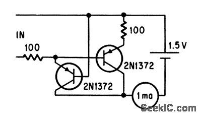
Substitution of transistors for diodes in rectifier circuit of a-c milliohm-meter gives significant increase in sensitivity and linearity. Uses inexpensive milliammeter.-P. Lefferts, Transistors Replace Diodes in Milliohmmeter Circuit, Electronics, 39:18, p 97. (View)
View full Circuit Diagram | Comments | Reading(3085)
Y_AMPLIFIER_FOR_CRO
Published:2009/7/10 21:45:00 Author:May
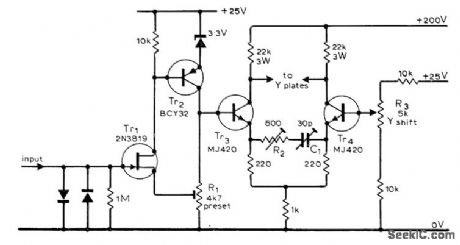
Combines advantages of differential output stage and high-impedance JFET input stage. Silicon input diodes provide crude overload protection for input, while Tr2 acts with Tr1 for level-shifting as well as amplifying. R1 is used to set quiescent output voltage of Tr2 at about 15 V; this setting is critical, and may require multitum pot. Article gives setup procedures.-G. A. Johnston, Deflection Amplifier for Oscilfoscopes, Wireless World, April 1975, p 175. (View)
View full Circuit Diagram | Comments | Reading(1132)
Heart_rate_monitor
Published:2009/7/17 4:34:00 Author:Jessie
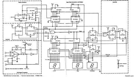
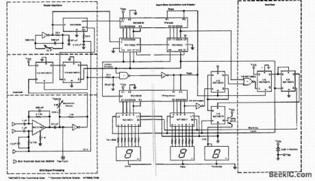
Heart rate monitor (courtesy Motorola Semiconductor Products Inc.). (View)
View full Circuit Diagram | Comments | Reading(4274)
05_W_AF_IC
Published:2009/7/10 21:44:00 Author:May
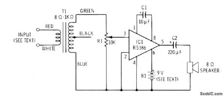
Simple audio power stage drives8-ohm loudspeaker for producing greater volume with pocket radio or for intercom applications. Supply range is 4-12 V. For long life, 6-V lantern batteries are recommended. Transformer is Radio Shack 273-1380.-F. M. Mims, Inteqrated Circuit Projects, Vol. 5, Radio shack;, Fort Worth, TX, 1977, 2nd Ed., p 38-44. (View)
View full Circuit Diagram | Comments | Reading(1886)
TELEPHONE_TOLL_TOTALIZER
Published:2009/7/10 21:44:00 Author:May
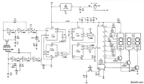
The Telephone loll Totalizer-built around two 4 518 dual synchronous up counters, a 74C925 4-digit counter, a 4 584 hex inverting buffer, and a 4081 quad 2-input AND gate-is fairly simple.Approximate toll charges can be calculated with this counter. It is started when dialing and stopped (manually) on hang-up. It is actually a counter that measures the time you are on the telephone. By calibrating it to the average cost/second of calls (get this from calculations you have done on your monthly phone bill), you can closely estimate your phone bill.The circuit consists of an oscillator running at the 100000 x frequency into the main counter (74C925). Typically, cost of telephone calls is 15 to 25 cents/minute so that the clock frequency (U1) is in the 25- to 40-kHz range. U2 and U4 with gates U3 form a ÷100000 counter. The approximate cost in dollars and cents is read out on the multiplexed display, DISP 1, 2, 3. S2 resets the counter to zero after each use. (View)
View full Circuit Diagram | Comments | Reading(3238)
| Pages:802/2234 At 20801802803804805806807808809810811812813814815816817818819820Under 20 |
Circuit Categories
power supply circuit
Amplifier Circuit
Basic Circuit
LED and Light Circuit
Sensor Circuit
Signal Processing
Electrical Equipment Circuit
Control Circuit
Remote Control Circuit
A/D-D/A Converter Circuit
Audio Circuit
Measuring and Test Circuit
Communication Circuit
Computer-Related Circuit
555 Circuit
Automotive Circuit
Repairing Circuit