
Circuit Diagram
Index 816
BANDSWITCHED_GRID_DIP_METER
Published:2009/7/10 5:20:00 Author:May

For checking resonances,tuned circuits,antennas,etc.this circuit covers the 2-to 20-MHz range.Q1 serves as an oscillator tunable over this range vta C1 and bandswitched coils L1 through L8.When theprobe is coupled to a circuit resonant at the oscillation frequency,some RF power will be absorbed andtheoscillator output will drop,Q2,D2,D3,and Q3 form an RE detector and dc amplifier to drive meter M1,which will show the drop in Rf level,indicating resonance.R2 is a sensitivity control. (View)
View full Circuit Diagram | Comments | Reading(1304)
Weighted_averaging_amplifier_using_half_of_an_ECG947_dual_operational_amplifier
Published:2009/7/19 21:06:00 Author:Jessie
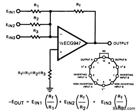
Weighted averaging amplifier using half of an ECG947 dual operational amplifier. The ECG947 is short-circuit protected and requires no external components for frequency compensation (courtesy GTE Sylvania Incorporated). (View)
View full Circuit Diagram | Comments | Reading(608)
30_MC_DOUBLE_TUNED
Published:2009/7/10 5:19:00 Author:May
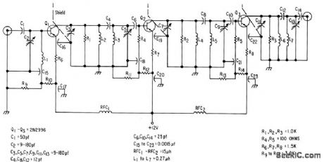
Proper loading provides good stabilily along with gain of 21 db per stage,despite inherent instability of 2N2996 at this frequency. Total power gain is thus 63 db, for noise figure of 2.3 db and bandwidth of 3 Mc.-Texas Instruments Inc., solid-Stale Communications, McGraw-Hill,N.Y, 1966, p 310. (View)
View full Circuit Diagram | Comments | Reading(635)
5V_AT_200mA
Published:2009/7/19 21:06:00 Author:Jessie
Article gives step-by-step design procedure for developing special opamp regulator when commercial unit meeting desired specifications is not available. Opamp is μA741. Circuit gives good regulation along with short-circuit protection, with less than 2 mV P-P AC ripple. Required input of 20V is obtained from conventional full-wave bridge rectifier with capacitor-input filter.-C. Brogado, IC 0p Amps Simplify Regulator Design, EDN/EEE Magazine, Jan. 15, 1972, p 30-34. (View)
View full Circuit Diagram | Comments | Reading(804)
BOXCAR_DETECTOR
Published:2009/7/19 21:05:00 Author:Jessie
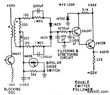
Diodes conduct during range gate interval of 0.2 microsec in portable doppler radar, to connect video signal to filter circuit.-J. Scott, D. Randise, and R. P. Lukacovic, Portable Radar Traces Battlefield Deployment, Electronics, 33:12, p 67-70. (View)
View full Circuit Diagram | Comments | Reading(662)
DIVIDE_BY_N_1_2_CIRCUIT
Published:2009/7/10 5:18:00 Author:May
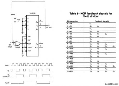
This circuit, instead of dividing by an integer, divides the input signal by N+1/2. With the feedback connections exactly as the figure shows, the circuit divides by 3.5. Point C ultimately controls when the input clocks the 74HC1614-bit counter. When C=0, the positive edge of the input triggers the counter. If C=1, the negative edge of the input triggers the counter. Each time that point C changes level, the circuit shortens the output pulse width of the counter by half of an input cycle. Thus, the counter's divisor depends on how many changes occur at point C during one output period.
Although the figure divides by 3.5, feeding back different counter outputs produces different divisors. Generally, an m-bit binary counter with pure exclusive-OR (XOR) feedback can form an N+1/2 counter, where N ranges from 2m-2+1/2 to 2m-1/2. The divided output is available at the m-1 bit of the counter. (View)
View full Circuit Diagram | Comments | Reading(1196)
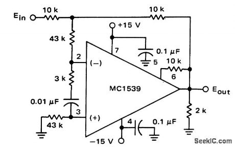
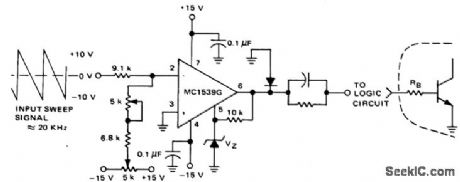
Differential_amplifier_with_low_noise_output_using_an_MC1539_op_amp_
Published:2009/7/19 21:05:00 Author:Jessie
Differential amplifier with low-noise output using an MC1539 op amp (courtesy Motorola Semiconductor Inc.). (View)
View full Circuit Diagram | Comments | Reading(821)
BOOTSTRAPPED_FET_SOURCE_FOLLOWER
Published:2009/7/10 5:18:00 Author:May
Gives 6 db gain for high-impedance transducer output, when 5-meg gate bias resistor is bootstrapped to the source through 100-mfd electrolytic.-L. J. Sevin, Jr., Field-Effect Trclnsislors, Mc Graw-Hill, N.Y., 1965, p 67. (View)
View full Circuit Diagram | Comments | Reading(1140)
Unity_gain_op_amp_with_fast_response_time
Published:2009/7/19 21:05:00 Author:Jessie
Unity-gain op amp with fast response time(courtesy Motorola Semiconductor Products Inc.). (View)
View full Circuit Diagram | Comments | Reading(839)
A_C_COUPLED_CASCODE
Published:2009/7/10 5:18:00 Author:May
Circuit is uniquely suited to inerectsing bandwidth of low-noise amplifier by reducing miller effect and per mining independent adiustment of operating conditions for optimum noise performance,-Texas Instruments Inc., Solid-Stale Communications, Mc Graw-Hill, N.Y.1966, p 143. (View)
View full Circuit Diagram | Comments | Reading(664)
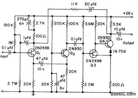
VARIABLE_DUAL_POLARITY
Published:2009/7/19 21:05:00 Author:Jessie
External resistor R0 determines values of positive and negative regulated output voltages provided by Silicon General SG3501 dual regulator.-H. Olson, Second-Generation IC Voltage Regulators, Ham Radio, March 1977, p 31-37. (View)
View full Circuit Diagram | Comments | Reading(993)
BLOCKING_OSCILLATOR_FOR_10_1_SYNC
Published:2009/7/19 21:04:00 Author:Jessie
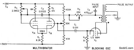
Combines basic mvbr and blocking oscillator into self-gated oscillator that gives synchronization ratio of 10:1 or greater, with stability equal to that of conventional circuit having 1:1 synchronization.-W. W. Whatley Blocking Oscillator for Ten-to-One Sychronization, Electronics, 32:48, p 58-59. (View)
View full Circuit Diagram | Comments | Reading(871)
AF_OUTPUT
Published:2009/7/10 5:17:00 Author:May
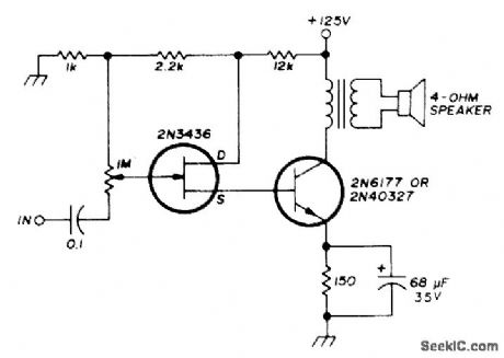
Operates directly from 125-V rectified AC line voltage. Combination of unipolar and bipolar transistors gives desirable amplifying features of each solid-state device.-I. M.Gottlieb, A New Look at Solid-State Amplifiers, Ham Radio, Feb. 1976 p 16-19. (View)
View full Circuit Diagram | Comments | Reading(1047)
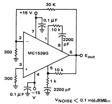
Voltage_comparator_using_an_MC1539G_op_amp
Published:2009/7/19 21:04:00 Author:Jessie
Voltage comparator using an MC1539G op amp (courtesy Motorola Serniconductor Products Inc.). (View)
View full Circuit Diagram | Comments | Reading(630)
AUDIO_VIDEO_SWITCHER
Published:2009/7/10 5:14:00 Author:May
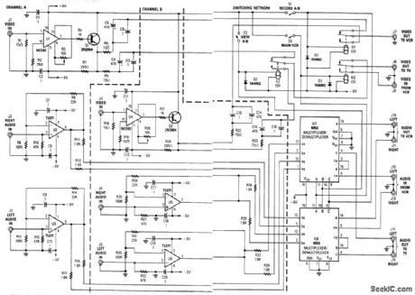
This circuit is a two-channel baseband video switcher. Buffer amps U1/Q1, U4/Q4, and associated components produce a buffered 75-Ω video signal, which is routed to switching network K1/K2/K3. Relay K1 selects either of these two video amplifiers and feeds J7. K2 also routup of either video amplifier to K3, which passes the selected video channel to J8 or connects J9 to J8.U2 andJ3 are audio amplifiers,which drive U7 and J8(CD4053 analog switches)to route audio from J1 and J2 to either J14/J15,or J10/J11.Also,audio from J12/J13 can be routed to these jacks.
(View)
View full Circuit Diagram | Comments | Reading(3492)
SINGLE_IC_WITH_TRANSFORMERS
Published:2009/7/10 5:14:00 Author:May
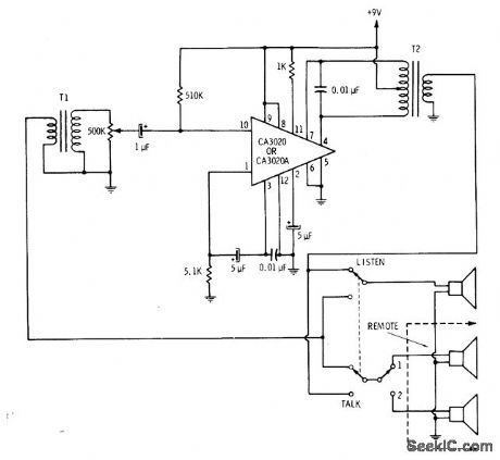
CA3020 differential amplifier uses AF input transformer T1 to matchloudspeakers(used as microphone) to higherinput resistance of IC,AF outputtransformer T2 similarly matches IC to loudspeakers operating conventionally.-E. M. Noll, Linear IC Principles, Experiments, and Projects, Howard W. Sams,Indianapolis,IN, 1974, p 100-101. (View)
View full Circuit Diagram | Comments | Reading(1007)
PUSHBUTTON_CONTROLLED_POWER_SWITCH
Published:2009/7/10 5:13:00 Author:May
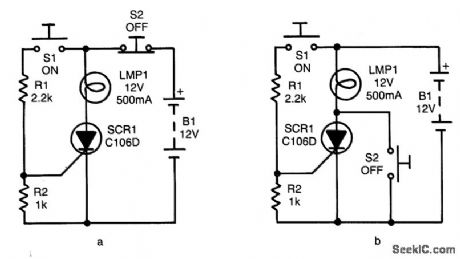
In both circuits, the SCR (and thereby the lamp) can be latched on by momentarily closing S1, thereby feeding gate drive to the SC via R1. In both circuits, the gate is tied to the cathode via R2 to improve circuit stability.Of course, after the SCR turns on, it can be tumed off again only by momentarily reducing anode current below the device's IH value. The SCR is tumed off by momentarily opening S2, by using S2 to short the anode and cathode terminals of the SCR momentarily. (View)
View full Circuit Diagram | Comments | Reading(1045)
High_impedance_high_gain_inverting_amplifier
Published:2009/7/19 21:03:00 Author:Jessie
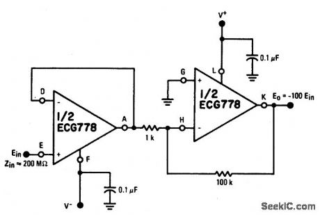
Typical supply voltages are +15 volts and -15 volts (courtesy GTE Sylvania Incorporated). (View)
View full Circuit Diagram | Comments | Reading(1094)
PRF_GENERATOR_1
Published:2009/7/19 21:03:00 Author:Jessie
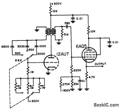
Blocking oscillator operates in range of 200 to 2,000 pps, as radar repetition-rate generator having frequency stability of about 5%. Has positive grid return, although this may decrease frequency stability if heater voltage drops below rated value.-NBS, Handbook Preferred Circuits Navy Aeronautical Electronic Equipment, Vol. 1, Electron Tube Circuits, 1963, p N5-2. (View)
View full Circuit Diagram | Comments | Reading(0)
OP_AMP_POWER_DRIVER
Published:2009/7/10 5:13:00 Author:May
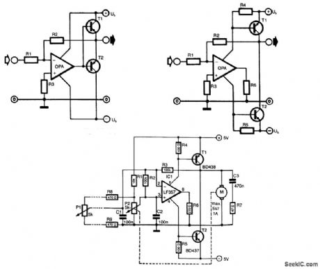
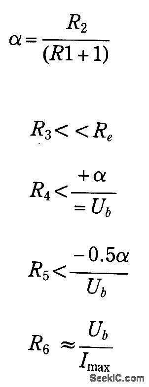
Frequently, the output current of an operational amplifier is inadequate for the application as, for instance, when a small motor or loudspeaker has to be driven. Normally, this is resolved by adding an emitter follower to the circuit as shown in Fig. 27-1(a). Unfortunately, that circuit does not allow the full supply voltage, Ub, to be used, because the output voltage of the op amp must always be 1 to 2 V smaller than ± Ub. To that must be added the drop across the base-emitter junction of transistors T1 and T2.
The circuit shown in Fig. 27-1(b) (principle) and Fig. 27-1(c) (practical) is a more appropriate solu-tion: it was designed specifically for driving small motors. Since the output current of the op amp flows through its supply lines, the driver transistors may also be controlled over these lines.
The value of base-emitter resistors R4 and R5 has been chosen to ensure that in spite or the quiescent current through the op amp, T1 and T2 are switched off. Resistor R6 limits the output current of the op amp. If the op amp is a type with guaranteed short-circuit protection, R6 may be replaced by a jump lead.
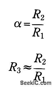
The output voltage is only 50 to 100 mV (collector-emitter saturation voltage of the driver transistors) smaller than the supply voltage. When choosing these transistors, it is therefore essential to take into account the saturation voltage (in addition to the maximum current amplification and power rating).The value of the resistors in an Inverting circuit is calculated from:
where α is the amplification.
In a noninverting circuit (R1 between the -input and ground and the input signal connected to the +input of the op amp), the amplification is:
where Re is the input impedance of the op amps.
The circuit can be used with discrete (single) op amps only, because double or quadruple types in one package share the supply voltage pins. The setting accuracy of the circuit in Fig. 27-1(c) is better than 1%. (View)
View full Circuit Diagram | Comments | Reading(986)
| Pages:816/2234 At 20801802803804805806807808809810811812813814815816817818819820Under 20 |
Circuit Categories
power supply circuit
Amplifier Circuit
Basic Circuit
LED and Light Circuit
Sensor Circuit
Signal Processing
Electrical Equipment Circuit
Control Circuit
Remote Control Circuit
A/D-D/A Converter Circuit
Audio Circuit
Measuring and Test Circuit
Communication Circuit
Computer-Related Circuit
555 Circuit
Automotive Circuit
Repairing Circuit