
Circuit Diagram
Index 987
CRYSTAL_TIMEBASE
Published:2009/7/7 7:12:00 Author:May
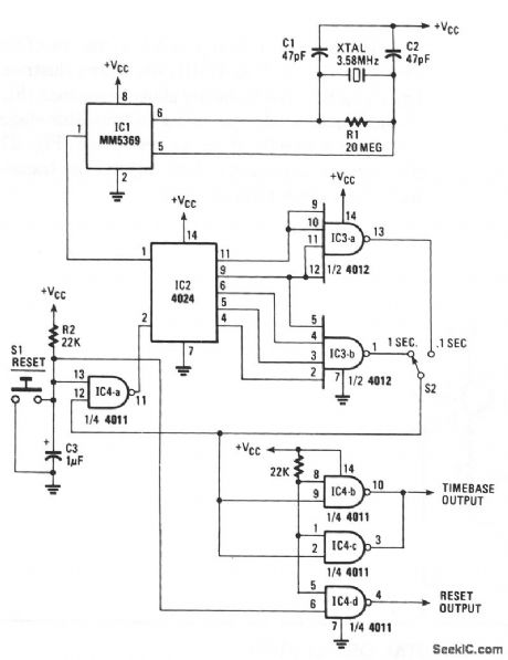
An on-board oscillator and a 17-stage divider compose IC1. By connecting a standard 3.58-MHz, television color-burst crystal as shown, an accurate source of 60-Hz squarewaves is generated at the IC's output, pin 1. Those pulses are then fed to IC2, a 4024 seven-stage ripple counter. Its outputs are connected to different gates in IC3, which is a dual four-input NAND gate. Depending on which position pulse-select switch S2 is on, one of those gates will provide an output/reset pulse of the selected width. (View)
View full Circuit Diagram | Comments | Reading(1349)
SIMPLE_CMOS_CRYSTAL_OSCILLATOR
Published:2009/7/7 7:10:00 Author:May
The circuit is an inverter set up as a linear amplifier. Adding the crystal and capacitors to the feedback path, we tum the amplifier into an oscillator and force it to oscillate at, or least very near, the crystal's resonant frequency. Trimmer capacitor C2 adjusts the actual operating frequency of the circuit. The crystal should be a parallel-resonant type; maximum frequency will depend partly on supply voltage, but it should be possible to go to at least 1 MHz. (View)
View full Circuit Diagram | Comments | Reading(2288)
GAS_SMOLE_DETECTOR
Published:2009/7/7 7:10:00 Author:May
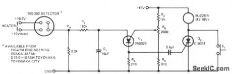
The sensor is based on the selective absorption of hydrocarbons by an n-type metal-oxide surface. The heater in the device serves to burn off the hydrocarbons once smoke or gas is no longer present in the immediate area; hence, the device is reuseable. When initially turned on, a 15 minute warm-up period is required to reach equilibrium (VA ≌ 0.6 V) in a hydrocarbon-free environment. When gas or smoke is introduced near the sensor, VA will quickly rise (rate and fmal equilibrium depend on the type of gas and concentration) and trigger Q1, a programmable unijunction transistor. The voltage pulse generated across R4 triggers Q2, sounding the buzzer until S1 resets the unit. R1 and C1 give a tiine delay to prevent small transient waves of smoke, such as from a cigarette, from triggering the alarm. Triggering threshold is set by R5, R2, and R3; with the components shown, between 50 and 200 ppm of hydrocarbons can be easily detected. Since it is somewhat sensitive to heater voltage, a regulated supply should be used. Power requirements are 1.5 V at 500 mA for the heater and 15 V at 30 mA, depending on type of buzzer, for the bias supply. (View)
View full Circuit Diagram | Comments | Reading(836)
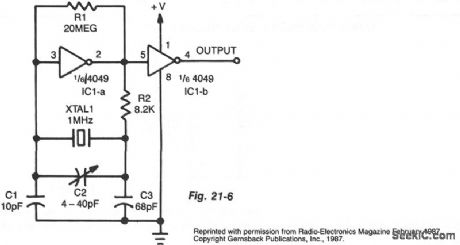
1_MHz_PIERCE_OSCILLATORS
Published:2009/7/7 7:09:00 Author:May
Simple network design is a key feature of the Pierce circuit, as these 1-MHz oscillators illustrate .Operating the crystal slightly above resonance (Fig.21-5a) requires only one high-gain transistor stage.Operating it exactly at series resonance (Fig. 21-5b) requires an extra RC phase lag and two transistors which can have lower gain. (View)
View full Circuit Diagram | Comments | Reading(2567)
SMOKE_GAS_VAPOR_DETECTOR
Published:2009/7/7 7:07:00 Author:May
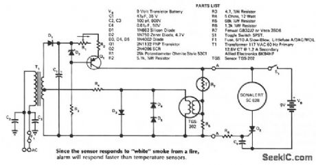
Transformer T1 supplies power to the heater of the sensor. Since the sensor is fairly sensitive to heater voltage, diodes D3, D4, and D5 regulate the heater voltage. T1, together with D1 and C2, forms a dc power supply, whose current is regulated by Q1 and adjusted by R1. The constant current from Q1 feeds a variable resistance, consisting of thermistor R7 and the parallel combination of R5 and the sensor resistance. When a hazard causes the voltage at A-A to drop, the net voltage at the SCR gate turns posi-tive, triggering the SCR on and operating the alarm. The alarm draws a small amount of current, so the battery will last a long time. Switch S1 turns off the alarm and resets the SCR. (View)
View full Circuit Diagram | Comments | Reading(847)
EASY_START_UP_CRYSTAL_OSCILLATOR
Published:2009/7/7 7:06:00 Author:May
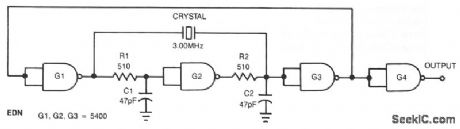

This low cost, crystal-controlled oscillator uses one TTL gate. Two factors ensure oscillator start-up: The connection of NAND gates G1, G2, and G3 into an unstable logic configuration and the high loop gain of the three inverters. Values of R1, R2, C1, and C2 aren't critical; select them so the oscillator operates at a frequency 70 to 90% higher than the crystal frequency when the crystal is disconnected. For 1-2 MHz operation, a low-power 54L00IC is recommended; for a 2-6 MHz, a standard 5400 type; and for 6-20 MHz, a 54H00 or 54S00.
(View)
View full Circuit Diagram | Comments | Reading(899)
METHANE_CONCENTRATION_DETECTOR_WITH_LINEARIZED_OUTPUT
Published:2009/7/7 7:05:00 Author:May
View full Circuit Diagram | Comments | Reading(935)
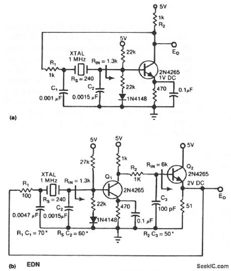
FUNDAMENTAL_FR_EQUENCY_CRYSTAL_OSCILLATOR_2_60_PF_Qopendingon_Frquoncy_FREQUENCY_RANGE__1_0_N
Published:2009/7/7 7:04:00 Author:May
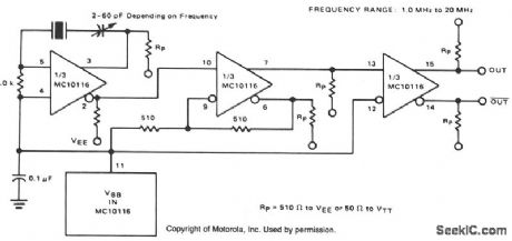
For frequencies below 20 MHz, a fundamental-frequency crystal can be used and the resonant tank is no longer required. Also, at this lower frequency range the typical MECL 10,000 propagation delay of 2 ns becomes small compared to the period of oscillation, and it becomes necessary to use a noninverting output. Thus, the MC10116 oscillator section functions simply as an amplifier. The 1.0 KΩ resistor biases the line receiver near VBBand the 0.1-μF capacitor is a filter capacitor for the VBB supply. The capacitor, in series with the crystal, provides for minor frequency adjustments. The second section of the MC10116 is connected as a Schmitt-trigger circuit; this ensures good MECL edges from a rather slow, less than 20-MHz input signal. The third stage of the MC10116 is used as a buffer and to give complementary outputs from the crystal oscillator circuit. The circuit has a maximum operating frequency of approximately 20 MHz and a minimum of approximately 1 MHz; it is intended for use with a crystal which operates in the fundamental mode of oscillation. (View)
View full Circuit Diagram | Comments | Reading(1491)
SMOKE_DETECTOR
Published:2009/7/7 7:03:00 Author:May
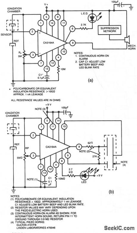
Use CA3164A BiMOS detector/alarm system. For operation as smoke detector with electromechan-ical horn (Fig. 40-1a), the output of driver at terminal8 is used. Large npn transistor Q3, with an active pull-up and transistor Q2 provide over 300 mA of drive current. For operation as a smoke detector with a piezoelectric ham (Fig. 40-1b), the circuit requires output from a second inverting amplifier at terminal 10, as well as the output from terminal 8. (View)
View full Circuit Diagram | Comments | Reading(0)
ELECTRONIC_DICE
Published:2009/7/7 7:00:00 Author:May
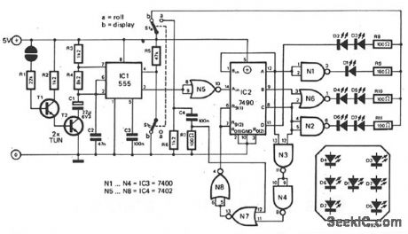
The basic die circuit is given. A 555 timer, IC1, is connected as an astable multivibrator. This feeds clock pulses to divide-by-six counter IC2 the outputs of which are decoded by gates N1 to N6 to drive an array of LEDs in the familiar die pattern. When switch S1 is in position b, the reset input of IC1 decreases and the oscillator is inhibited. Power is fed to the LEDs via Slb so that the display is activated. When the die is rolled 'oy switching 51 to position a, the display is blanked. C4 is connected to positive supply via Sla, producing a short pulse which resets IC2 via N7 and N8. The reset input of IC1 is pulled high via R5, so the multivibrator begins to oscillate and feeds clock pulses to IC2 via NS. When S1 is switched back to position a, the multivibrator is again inhibited. Then, the counter stops and power is applied to the LEDs which display the value of the throw. (View)
View full Circuit Diagram | Comments | Reading(0)
COIN_FLIPPER
Published:2009/7/7 6:56:00 Author:May
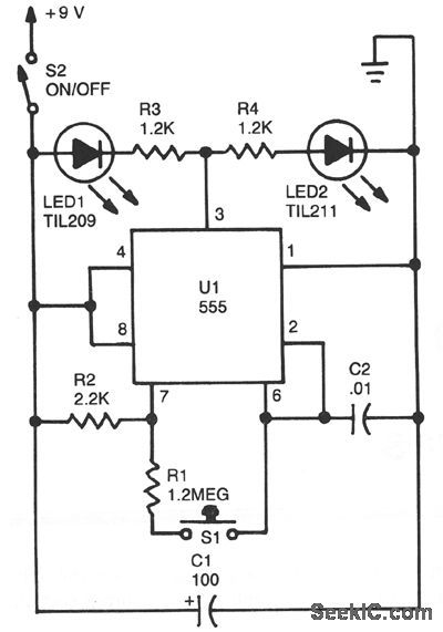
The circuit is basically a 555 astable circuit that divides two LEDs, LED1 and LED2. LED2 is switched on when the output of U1 is high, and LED1 is activated when its output is low. When U1 oscillates, LED1 and LED2 switch on alternately as the output of U1 switches from state to state. Resistor R1's value is high in comparison to R2, so the waveform at the output is a square wave with a mark/space ratio of nearly one-to-one. When you release S1, you break the circuit and U1 latches whatever the output state happens to be at the time. (View)
View full Circuit Diagram | Comments | Reading(1509)
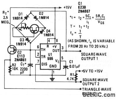
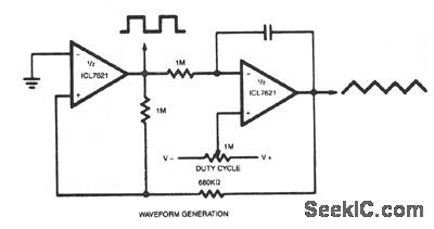
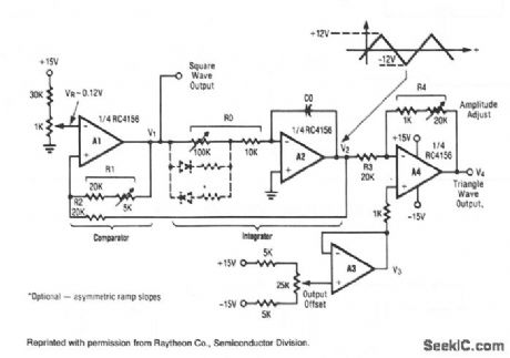
WIDE_RANGE_TRIANGLE__SQUARE_WAVE_GENERATOR
Published:2009/7/7 6:54:00 Author:May
View full Circuit Diagram | Comments | Reading(654)
PRECISE_TRIANGLE__SQUARE_WAVE_GENERATOR
Published:2009/7/7 6:52:00 Author:May
Since the output range swings exactly from rail to rail, frequency and duty cycle are virtually independent of power supply variations. (View)
View full Circuit Diagram | Comments | Reading(872)
SAWTOOTH_AND_PULSE_GENERATOR
Published:2009/7/7 6:51:00 Author:May

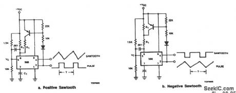
The pin 3 output of the 566 can be used to provide different charge and discharge currents for C1 so that a sawtooth output is available at pin 4 and a pulse at pin 3. The pnp transistor should be well saturated to preserve good temperature stability. The charge and discharge times can be estimated by using the formula:where RT is the combined resistance between pin 6 and VCC for the interval considered. (View)
View full Circuit Diagram | Comments | Reading(1609)
WIDE_RANGE_TUNABLE_FUNCTION_GENERATOR
Published:2009/7/7 6:49:00 Author:May
View full Circuit Diagram | Comments | Reading(700)
BASIC_FUNCTION_GENERATOR
Published:2009/7/7 6:48:00 Author:May
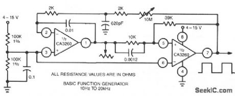
This function generator uses a CA3260 BiMOS Op amp to petform both the integrator and switchingfunctions.A 620-pF capacitor and 2-KΩ resistor shape feedback square wave to reduce spikes. Full audiospectrum, 10 Hz to 20 kHz,is covered with a single 10 Ω potentiometer. Requires 9-V battery. (View)
View full Circuit Diagram | Comments | Reading(870)
VARIABLE_DUTY_CYCLE_TIMER
Published:2009/7/7 6:46:00 Author:May

When configured as a free-running multivibra-tor, a 555 timer provides no more than a 50% duty cycle. By adding two transistors, however, you can obtain a variable 5 to 95% duty cycle without changing the sum of the on and off times. WhenVOUT decreases, Q1 is on and Q2 is off, disconnect-ing V+ while timing capacitor C2 discharges into pin 7 of the timer. When VOUT increases, Q2 reconnects V+ for recharging C2.Adjusting linear trimming potentiometer R3 to increase the charging resistance increases the on time, but decreases the off time by the same amount by lowering the discharge resistance (the converse is also true). As a result, the sum of the on and off times remains constant. R2 protects Q2 and the timer against high-charge/discharge currents. (View)
View full Circuit Diagram | Comments | Reading(2261)
TRIANGLE__SQUARE_WAVE_GENERATOR
Published:2009/7/7 6:44:00 Author:May
This circuit uses a positive-feedback loop closed around a combined comparator and integrator. When power is applied, the output of the comparator will switch to one of two states, to the maximum positive or maximum negative voltage. This applies a peak input signal to the integrator, and the integrator output will ramp either down or up, opposite of the input signal. When the integrator output, which is connected to the comparator input, reaches a threshold set by R1 and R2, the comparator will switch to the opposite polarity. This cycle will repeat endlessly, the integrator charging positive then negative, and the compara-tor switching in a square-wave fashion. (View)
View full Circuit Diagram | Comments | Reading(983)
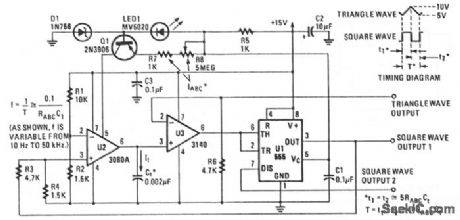
SINGLE_CONTROL_FUNCTION_GENERATOR
Published:2009/7/7 6:42:00 Author:May
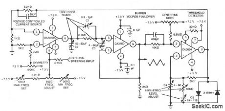

This function generator, with an adjustment range in excess of 1,000,000 to 1, uses a CA3160 BiMOS op amp as a voltage follower, a CA3080 OTA as a high-speed comparator, and a CA3080 as a programmable-current source. Three variable capacitors, C1, C2, and C3 shape the triangular signal between 500 kH and 1 MHz. Capacitors C4 and C5, and the trimmer potentiometer in series with C5, maintain essentially constant (±10%) amplitude to 1 MHz. (View)
View full Circuit Diagram | Comments | Reading(753)
ASTABLE_MULTIVIBRATOR
Published:2009/7/7 6:39:00 Author:May
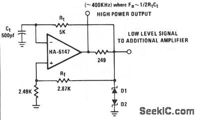
The power bandwidth of the HA-5147 extends the circuit's frequency range to approximately 500 kHz. Rt can be made adjustable to vary the frequency if desired. Any timing errors because of VOSorIbias have been minimized by the precision char-acteristics of the HA-5147. D1 and D2, if used, should be matched to prevent additional timing errors. These clamping diodes can be omitted by tying Rt and positive feedback resistor Rf directly to the output. (View)
View full Circuit Diagram | Comments | Reading(0)
| Pages:987/2234 At 209819829839849859869879889899909919929939949959969979989991000Under 20 |
Circuit Categories
power supply circuit
Amplifier Circuit
Basic Circuit
LED and Light Circuit
Sensor Circuit
Signal Processing
Electrical Equipment Circuit
Control Circuit
Remote Control Circuit
A/D-D/A Converter Circuit
Audio Circuit
Measuring and Test Circuit
Communication Circuit
Computer-Related Circuit
555 Circuit
Automotive Circuit
Repairing Circuit