
Circuit Diagram
Index 991
STEP_UP_DOWN_DC_DC_CONVERTER
Published:2009/7/7 5:27:00 Author:May
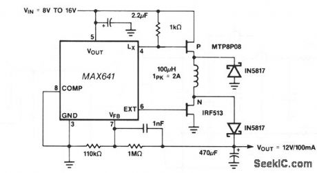
Positive output step-up and step-down dc-dc converters have a common limitation in that neither can handle input voltages that are both greater than or less than the output. For example, when converting a 12-V sealed lead/acid battery to a regulated + 12 V output, the battery voltage might vary from a high of 15 V down to 10V.
By using a MAX641 to drive separate P- and N-channel MOSFETs, both ends of the inductor are switched to allow noninverting buck/boost operation. A second advantage of the circuit over most boostonly designs is that the output goes to 0 V when shutdown is activated. Inefficiency is a drawback because two MOSFETs and two diodes increase the losses in the charge and discharge path of the inductor. The circuit delivers + 12 V at 100 mA at 70 percent efficiency with an 8-V input. (View)
View full Circuit Diagram | Comments | Reading(0)
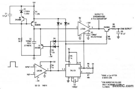
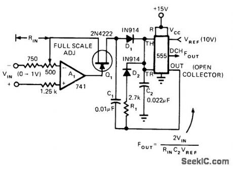
PULSE_WIDTH_TO_VOLTAGE_CONVERTER
Published:2009/7/7 5:25:00 Author:May
View full Circuit Diagram | Comments | Reading(1408)
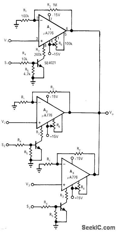
ANALOG_SUMMING
Published:2009/7/7 5:24:00 Author:May
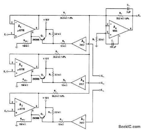
ON/OFF programming ofμA776 opamps allows any or all inputs to be on at given time. Switched outputs are combined in summing inverter A,. Voltage followers A1-A3 are programmed from on to off by Q1-Q3 and A5- A7. Noise gain of stage A4, is minimized when input channel is switched off. If sign inversion by A4, is undesirable, add inverter stage following A.. Any number of additional channels can be added. Programming pulses are applied to inputs of A,, A6, and A,.-W. G. Jung, IC 0p-Amp Cookbook, Howard W Sams, Indianapolis, IN, 1974, p 419-421. (View)
View full Circuit Diagram | Comments | Reading(790)
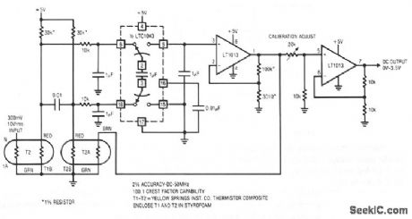
50_MHz_THERMAL_RMS_TO_DC_CONVERTER
Published:2009/7/7 5:23:00 Author:May
View full Circuit Diagram | Comments | Reading(1064)
VOLTAGE_RATIO_TO_FREQUENCY_CONVERTER
Published:2009/7/7 5:21:00 Author:May
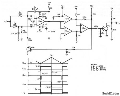
The circuit accents two positive-voltage inputs VN and VD and provides a TTL-compatible output pulse train whose repetition rate is Proportional to the ratio VN/VD. Full-scale output frequency is about 100 Hz,and linearity error is below 0.5 percent.The output F0 equals KVN/VD,where K=1/(4R2C1)provided R1=R3. Op amp ICIA alternately integrates VN/2 and - VN/2, producing a sawtooth cutou, that ramps between the VD level and ground.When transistor Q1 is on,for example, ICIA integrates -VN/2 until its Output equals VD. At that time, the IC1B comparator switches low, causing IClD's bistable output to go low, which turns off Q1. IClA's output then ramps in the negative direction. When the output reaches 0 V,the IC1C comparator switches,Q1 turns on,and the cycle repeats.Transistor Q2 converts the IC1D output to TTL-compatibl, output logic levels. Setting VD to 1.00 V yields a reciprocal voltage-to-frequency converter(Fo=KVN),and setting VN to 1.00 V yields a reciprocal voltage-to-frequency converter(Fo=KVD).
(View)
View full Circuit Diagram | Comments | Reading(969)
MULTIPLEXED_A_D_D_A_CONVERTER_INTER_FACE
Published:2009/7/7 5:20:00 Author:May

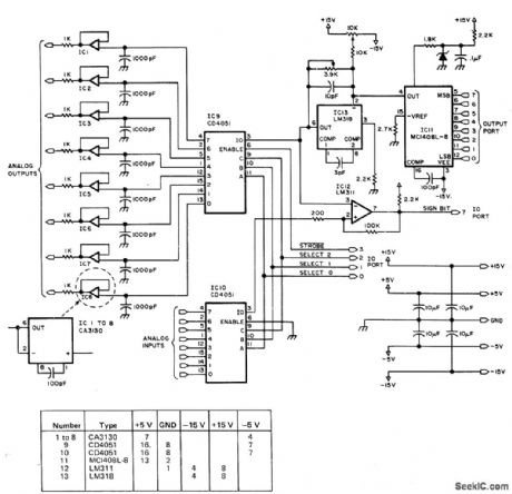
Time-multiplexed interface minimizes hardware required for applications of personal computer system. Useful in interactive games, equipment testing, and electronic music. Optimized for 0.1-100 Hz signals, Bypass each power pin with 0.01μF to suppress stray spikes caused by power surges. Use of LM318 opamp minimizes response time of MC1408L-8 DAC.-D. R. Kraul, Designing Multichannel Analog Interfaces, BYTE, June 1977, p 18-23. (View)
View full Circuit Diagram | Comments | Reading(2370)
TWO_INPUT_FSK_MULTIPLEXER
Published:2009/7/7 5:15:00 Author:May
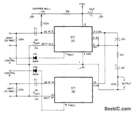
Uses Signetics NE571 or NE570 analog compandors. Gain of each channel is unity, as determined by RGAIN value for channel. When complementary control signals are provided, FSK generator switches between the two signal inputs. Outputs, when on, are summed by opamp in IC. Each channel is gated off by low control logic input. For FSK or alternate-channel ';'' C0N-TR0L A and CONTROL B signals should be com plementary. Control signal suppression is optimized with chopper null pot. Suppression is better than 60 dB after trimming. Circuit can also be used as summing switch, with both signals on at any given instant.-W. G. Jung, Gain Control IC for Audio Signal Processing, Ham Radio, July 1977, p 47-53. (View)
View full Circuit Diagram | Comments | Reading(1379)
EIGHT_CHANNEL_TELEMETER
Published:2009/7/7 5:11:00 Author:May
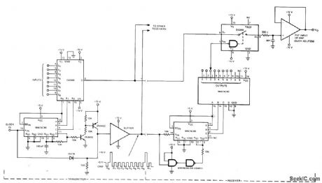
Multiplex transmission system permits monitoring eight different inputs at remote location, 5-V pulse train is sent down separate channel to receiving location to perform timing and synchronizing functions for outputs of MM74C42 BCD-to-decimal decoder. 15-V reset pulse is superimposed on 5-V clock. Other receivers can be added if monitoring is desired at more than one location.- Analog Switches and Their Applications, Siliconix, Santa Clara, CA, 1976, p 7-71-7-72. (View)
View full Circuit Diagram | Comments | Reading(1044)
10_V_TEMPERATURE_STABILIZED
Published:2009/7/7 5:10:00 Author:May
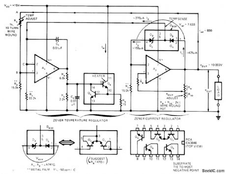
Self-regu lation of substrate temperature of CA3046 fivetransistor chip allows 10-V reference output voltage to rlse only 0.5 mV when temperature increases from 27 to 62℃ Circuit requires only single 15-V supply Zener-connected transistor Q2 and diode-connected transistor Q1 together provide temperature compensation by sensing voltage across Q1 (DS) and comparing it with temperature-reference voltage produced across R1 by μA741G opamp A1. Opamp drives Q5 to control current through Q4 which serves as chip heater. Opamp A2 (μA741G) and asso-ciated components (including Q1-Q2 in feedback path) act as self-regulating (zener-current) voltage reference.-M. J. Shah, A Self-Regutating Temperature-Sta bil ized Reference, EDN Maga-zine, May 20, 1974, p 74 and 76. (View)
View full Circuit Diagram | Comments | Reading(1900)
TRANSISTORS_FOR_DRIVER_TUBES
Published:2009/7/7 5:08:00 Author:May
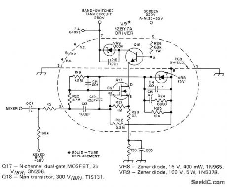
Solidstate replacement for 12BY7A power amplifier runs much cooler than tube. Shield is required between input and output circuits. Gate 2 is biased very high and gate 1 is close to source voltage, to permit maximum signal range with-out changing parameters. Bypassed zener VR9 prevents 100-V collector signal swing from exceeding transistor breakdown voltage. Solidstate replacements for other tube types in Drake T-4XB transmitter are also given in arti-cle.-H. J. Sartori, Solid-Tubes-a New Life for Old Designs, 057, April 1977, p 45-50. (View)
View full Circuit Diagram | Comments | Reading(1770)
MULTIPLEXING_OF_DISPLAYS
Published:2009/7/7 5:06:00 Author:May
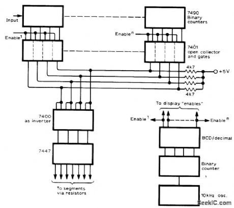
Three or more displays can be multiplexed simply by gating 7490 counter output via 7401, then using OR connection for outputs. 7401s are switched on in rotation by positive enable signal which also switches displays on in turn. If using common-cathode displays, segment and display enable signals must be inverted. With individual display units, segments must be paralleled.-G. A. Bobker, Simplified Multiplexing, Wireless World, Feb. 1978, p 59. (View)
View full Circuit Diagram | Comments | Reading(1024)
MODEL_RAILROAD_SWITCHING_
Published:2009/7/7 5:05:00 Author:May
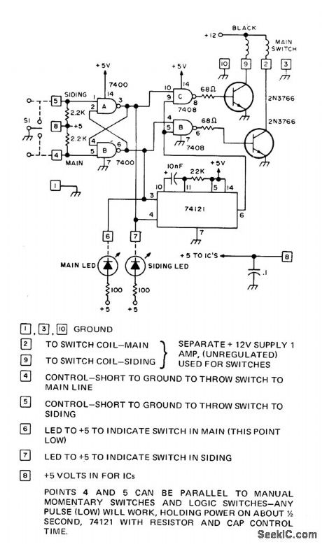
Control circuitis used to drive solenoid-operated track Switches oftγpical HO train layout Inputcan be ρair of comρlementary TTL signals from 8008 orother computer or can be from manual switch s1. 74121 mono MVBR controls time that witch is energized in given direction. Outputcult transistors are rated at 20 W,enough for driving solenoids taking 1 A at 12 V Use protective diodes across coils of solenoids,-H,De Monstoy,Model Railroad Switch Control Circuit,BYTE,Oct .1975,p 87. (View)
View full Circuit Diagram | Comments | Reading(962)
0_360°to_0_180°
Published:2009/7/7 5:05:00 Author:May
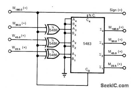
Used for converting angular information in 36O° wrap-around code to ±180°sign-plus-magnitude code. For values under 180°, converter outputs and inputs are identical. For larger input angles, output code is complement of input plus one. Used for interfacing shaft encoders and synchro-to-digital converters to digital display. Article gives truth table showing which lines are high and which are low at input and at output for angular increments of 22.5°.-J. N. Phillips, Convert Wrap-Around Code to Sign-Plus-Magnitude, EDN Magazine, Jan. 5, 1973, p 103. (View)
View full Circuit Diagram | Comments | Reading(604)
TEN_BAND_GRAPHIC_EQUALIZER,USING_ACTIVE_FILTERS
Published:2009/7/7 5:04:00 Author:May
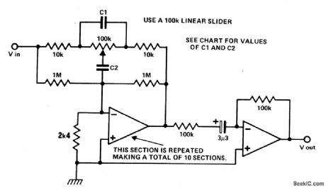


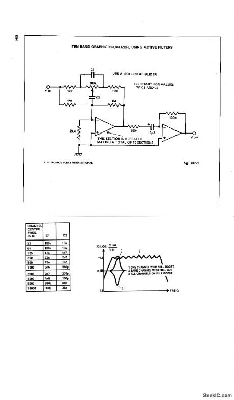
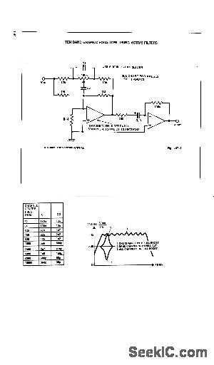
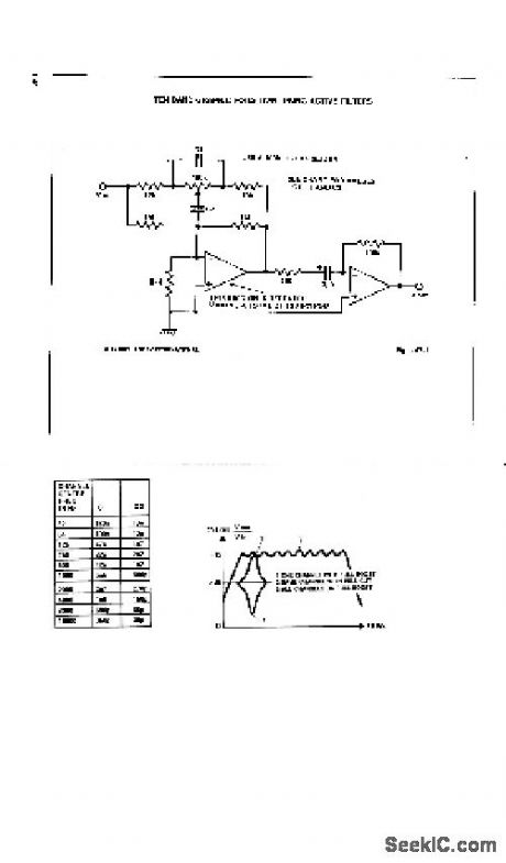
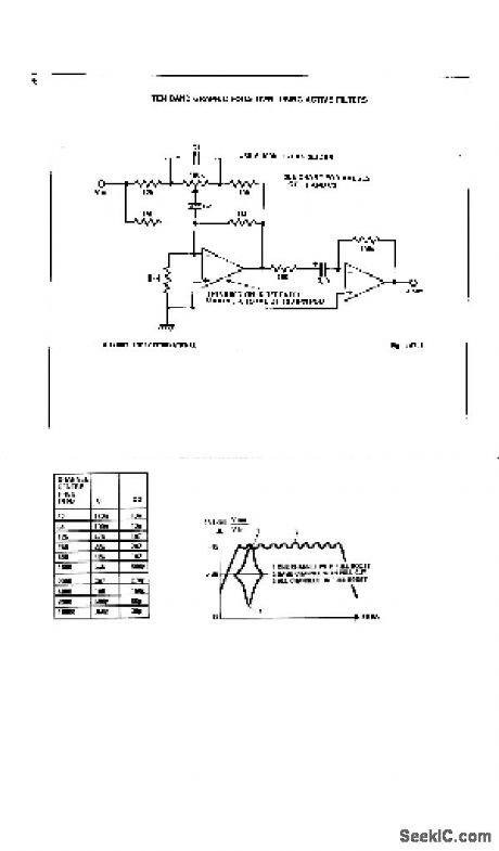
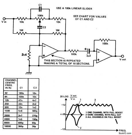
The above circuit is repeated ten times. Use the table to calculate values. (View)
View full Circuit Diagram | Comments | Reading(696)
LOGIC_SIGNALS_CONTROL_TDM
Published:2009/7/7 5:03:00 Author:May
se of μA776 opamps eliminates need for FET switches in time-division multiplexing and signal conditioning. Multiplex inputs S1-S2-S3 can be driven directly by TTL or DTL devices. Each amplifier is controlled by either supplying or denying its 70-μA master-bias input, thus turning it on or off. All stages have identical component values.-M. K. Vander Kooi, Multiplexing Without FETs, EDN/EEE Magazine, Aug. 1, 1971,p47. (View)
View full Circuit Diagram | Comments | Reading(719)
Solid_state_time_delay
Published:2009/7/22 3:48:00 Author:Jessie
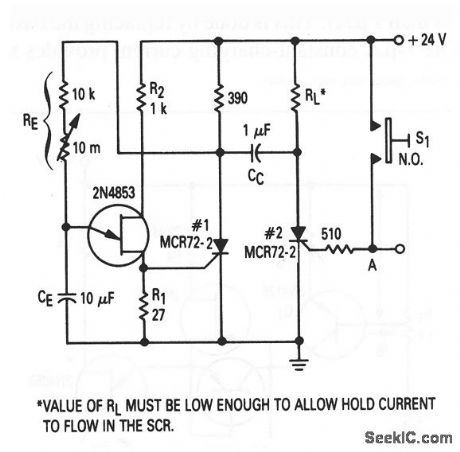
This circuit shows the basic UJT building block (Fig. 9-1), which is used to provide a time-delay function. The circuit is similar to that of Fig. 9-13, except that the mechanical relay is replaced by an SCR (which generally reduces circuit cost). When S1 is pushed, or when a positive-going pulse is applied at point A, SCR#2 turns on and SCR#1 is turned off by CC. With SCR#1 off, the supply voltage is applied to RE, and the circuit begins to time. After a period (determined by the setting of RE), the UJT fires and turns SCR#1 on and SCR#2 off. With the values shown, time delay can be varied from about 1 s to over 2 min. (View)
View full Circuit Diagram | Comments | Reading(1090)
_TONE_CONTROL
Published:2009/7/7 5:03:00 Author:May


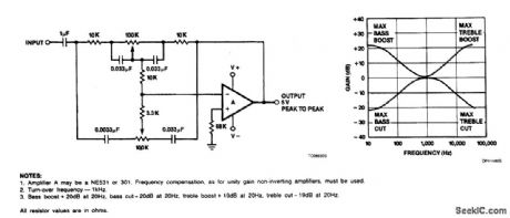
Tone control of audio systems involves altering the flat response ul order to attain more low frequenctes or more high ones,ependent upon listener preference.The circuit provides 20 dB of bass or treble boost or cut as set by the variable resistance.The actual response of the circuit is shown also.
(View)
View full Circuit Diagram | Comments | Reading(1207)
JFET_VFO
Published:2009/7/22 3:47:00 Author:Jessie
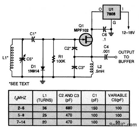
This circuit is a simple JFET-based, variable-frequency oscillator that can be used in receiver or transmitter circuits. The circuit is very stable; hence, if good-quality components and appropriate construction techniques are used, there will be very little drift in frequency. The component values listed in the table will give you a starting point to set up the oscillator to cover a desired frequency range. Inductor L1 is wound on a T50-6 toroidal core using #26 or #28 enamel-coated copper wire. The oscillator's frequency can be increased a small amount by removing a turn from the coil's winding; by the same token, the frequency can be decreased by adding a turn or two. After you have achieved the desired frequency range, cover the coil with a clear plastic coating or coil dope to keep the coil wires from moving around and causing the oscillator's frequency to shift. (View)
View full Circuit Diagram | Comments | Reading(4062)
0_10VDC_TO_0_10_kHz
Published:2009/7/7 5:03:00 Author:May
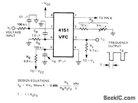
Single-supply voltage-to-frequency convener produces square-wave output at frequency varying linearly with input voltage. Linearity error is typically only 1%. For values shown, response time for step change of input from 0 to +10V is 135 ms. Uses Raytheon 4151 converter. Supply can be 15 V.- Linear Integrated Circuit Data Book, Raytheon Semi-conductor Division, Mountain View, CA, 1978, p7-38. (View)
View full Circuit Diagram | Comments | Reading(1151)
V_F_GIVES_10_to_10000_Hz
Published:2009/7/7 5:02:00 Author:May
Current proportional to input voltage is balanced via periodic charging of C1 to precisely repeatable voltage by opamp A1 and FET Q1. With values shown, nominal scale factor is 10 kHz/V, Input of0 to 1 V gives output of 10 to 10,000 Hz with better than 0.05% linearity. Article gives operating details and design equations.-W. S. Woodward, Simple 10 kHz V/F Features Differential Inputs, EDN Magazine, Oct. 20, 1974, p 86 (View)
View full Circuit Diagram | Comments | Reading(721)
| Pages:991/2234 At 209819829839849859869879889899909919929939949959969979989991000Under 20 |
Circuit Categories
power supply circuit
Amplifier Circuit
Basic Circuit
LED and Light Circuit
Sensor Circuit
Signal Processing
Electrical Equipment Circuit
Control Circuit
Remote Control Circuit
A/D-D/A Converter Circuit
Audio Circuit
Measuring and Test Circuit
Communication Circuit
Computer-Related Circuit
555 Circuit
Automotive Circuit
Repairing Circuit