
Circuit Diagram
Index 983
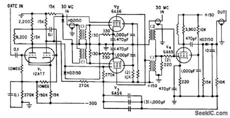
TV_IF_amplifier_uslng_dual
Published:2009/7/21 8:27:00 Author:Jessie
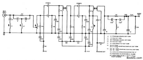
TV IF amplifier uslng dual-gate MOSFETs The IF response is as follows∶39.75 MHz greater than 30 dB down, 41.25 MHz greater than 40 dBdown,47.25 MHz greater than 30 dB down,42.17 nealy 8 dB down,45.75 MHz equalto 6 dB down.Senstivity is 700 μV for 1V of video carrier at 100% modulation.AGC range is 43 dB AGC voltage is +4.0 V to-6.0V.Sound output is 570μV of 4.5 MHz signal(courtesy Texas Instruments Incorporated).
(View)
View full Circuit Diagram | Comments | Reading(816)
Output_storage_register_using_an_ADC171_dual_slope_integrating_A_D_converter
Published:2009/7/21 8:25:00 Author:Jessie
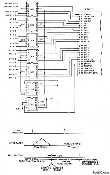
Output storage register using an ADC171 dual-slope integrating A/D converter (courtesy Analog Devices, Inc.). (View)
View full Circuit Diagram | Comments | Reading(845)
TRIGGER_WITH_TRANSMISSION_LINE_FEED_BACK
Published:2009/7/21 8:03:00 Author:Jessie
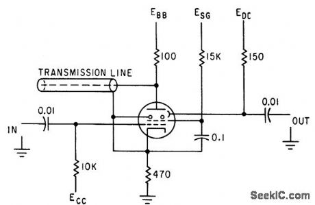
Feedback capacitor is replaced by open-circuited section of transmission line, Duration of output pulse taken across dynode load of secondary-emission penlode is adjusted by varying line length.-E. J. Martin, Jr., How to Use the Secondary-Emission Pentode, Electronics, 33:41, p 60-63. (View)
View full Circuit Diagram | Comments | Reading(650)
D_C_TRIGGER_DRIVES_HIGH_C_COAX
Published:2009/7/21 8:03:00 Author:Jessie
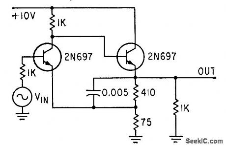
Emitter-follower incorporated in Schmitt circuit provides signal shaping needed to drive high-capacitonce cable with good rise time and few components.-G. Klein, Schmitt Trigger Drives Low Impedance Loads, Electronics, 36:33, p 28-29. (View)
View full Circuit Diagram | Comments | Reading(826)
CHOPPER_AND_PHASE_DETECTOR
Published:2009/7/21 8:01:00 Author:Jessie
Input gate signal operates Schmitt trigger V1, to give identical but oppositely phased signals for phase detector of instrument for measuring phase differences between two signals.-R. T. Stevens, Precision Phasemeter for CW or Pulsed UHF, Electronics, 33:10, p 54-57. (View)
View full Circuit Diagram | Comments | Reading(824)
PULSE_DELAY_WITH_DUAL_EDGE_TRIGGER
Published:2009/7/7 8:44:00 Author:May
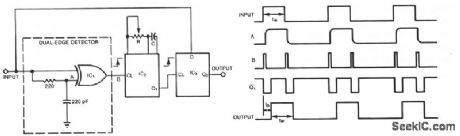
A single monostable multivibrator delays a pulse train by a variable amount; nonetheless, this amount can be no less than the minimum allowed pulse width tw The exclusive-OR gate, IC1, generates a short pulse following every leading or falling edge of the input waveform. These pulses cause one-shot IC2 to produce a negative-going pulse with a duration equal to the desired time delay tp which you set by adjusting potentiometer R. Flip-flop IC3 then creates a delayed replica of the input pulse by latching the Q1 out-put of IC2 between positive-going transitions. You can independently control the output-pulse duration by cascading a second one shot with the first. (View)
View full Circuit Diagram | Comments | Reading(904)
LEADING_EDGE_DELAY
Published:2009/7/7 8:42:00 Author:May
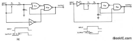
Circuit (a) lets you delay the leading edge of a positive pulse while leaving the trailing edge almost unaffected. A positive input transition, inverted by IC2, has no effect on IC1B. However, when the positive transition reaches IC1A, (delayed by the adjustable network of R1, R2, and C1), it toggles both NOR gates, initiating the output pulse. When the input decreases IC1B follows suit, delayed only by the propagation through itself and IC2. Circuit (b) produces an inverted output pulse. Inverter IC1 serves as a buffer for the signal source-an advantage when driving a low-impedance (short-delay) network. Moreover, only the propagation delay of IC2B separates the output's trailing edge from that of the input. You can configure circuit (a) to handle negative pulses by using NAND instead of NOR gates. Similarly, circuit (b) will produce a delayed positive pulse in response to negative input pulse, if you substitute NOR gates for NAND gates.
(View)
View full Circuit Diagram | Comments | Reading(840)
TV_video_signal_processor_circuit_2
Published:2009/7/21 8:00:00 Author:Jessie
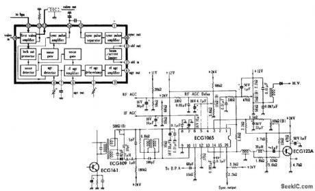
TV video signal processor circuit. The EGG 1065 is a 16-pin DIP (courtesy GTE Sylvania Incorporated). (View)
View full Circuit Diagram | Comments | Reading(701)
SOUND_CTIVATED_DECODER
Published:2009/7/7 8:40:00 Author:May
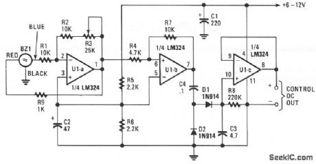
The piezo transducer operates as a sound-pickup device as well as a frequency-selective filter. By controlling the gain of the op amps, the oscillator can be transformed into a sensitive and frequency-selec-tive tone-decoder circuit. With the gain of U1a set just below the point of self oscillation, the transducer becomes sensitive to acoustically coupled audio tones that occur at or near its resonant frequency.
The circuit's output can be used to activate optocouplers, drive relay circuits, or to control almost any dc-operated circuit. The dc signal at the output of U1c varies with 0 to over 6 V, depending on the input-signal level. One unusual application for the sound-activated decoder would be in extremely high-noise environments, where normal broadband microphone pickup would be useless. Because piezo transducers respond only to frequencies within a very narrow bandwidth, little if any of the noise would get through the transducer. (View)
View full Circuit Diagram | Comments | Reading(1281)
VOLTAGE_LEVEL_TRIGGER
Published:2009/7/21 8:00:00 Author:Jessie
Output pulse appears when input is 6.0 v but not for inputs up to 7 volts above or below this level. Circuit then continues on until input drops below 5.4 v.-R. F. Woody, Precise 6-Volt Input Triggers Circuit, Electronics, 38:14, p 80. (View)
View full Circuit Diagram | Comments | Reading(1016)
DIRECTION_DETECTOR_DECODER
Published:2009/7/7 8:37:00 Author:May
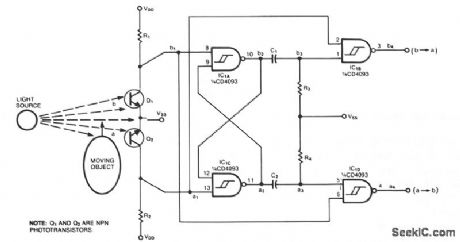
This circuit, which was developed to monitor the traffic of bumblebees in and out of the hive, differentiates a-to-b motion from b-to-b motion. When used with an optical decoder, the circuit distinguishes clockwise from counterclockwise rotation and provides a resolution of one output pulse per quadrature cycle.
Q1 and Q2 are mounted so that a moving object first blocks one phototransistor, then both, then the other. Depending on the direction in which the object is moving, either IC1B or IC1D emits a negative pulse when the moving object blocks the second sensor. An object can get as far as condition 3 and retreat without producing an output pulse; that is, the circuit ignores any probing or jittery motion. If an object gets as far as condition 4, however, a retreat will produce an opposite-direction pulse.
The time constants R3C1 and R4C2 set the output pulse width. A 100 K Ω/100pF combination, for example, produces 10-μs pulses. Select a value for pullup resistors R1 and R2 from the 10 K to 100 KΩ range, according to the sensitivity your application requires. (View)
View full Circuit Diagram | Comments | Reading(1999)
RESISTOR_TESTER
Published:2009/7/21 7:59:00 Author:Jessie
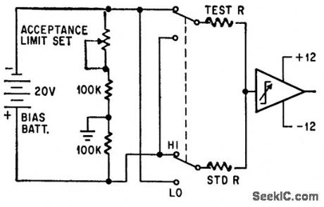
Operational trigger is tripped by bridge circuits when resistor under test is 0.11% high for switch position shown. Reversing switch gives same sensitivity for low resistors.-P. Lefferts, Operational Trigger For Precise Control, Electronics, 37:28, p 50-55. (View)
View full Circuit Diagram | Comments | Reading(746)
ENCODER_DECODER
Published:2009/7/7 8:36:00 Author:May
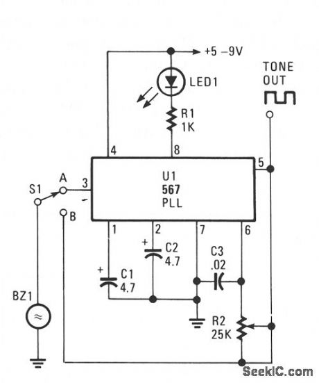
The transducer circuit can be operated as either a tone encoder or decoder by changing the position of S1. The operating frequency of that dual-purpose circuit is determined by C3 and R2.Capacitors C1 and C2 are not critical and can be of almost any value between 1 and 5 mf. When the circuit is receiving an on-frequency signal, LED1 lights. Although a two wire piezo transducer with a resonance frequency of 2500 Hz was used in the circuit, any piezo unit should work-as long as the values of C3 and R2 are selected to tune to the transducer's operating frequency.
With power on and S1 in the B position, adjust R2 for the loudest tone output. The circuit should be tuned to the resonance frequency of the trans-ducer. In that position, the circuit can be used as an acoustical or tone signal encoder. Next, switch to the A position and aim an on-frequency audible tone toward the transducer; the LED should light, indicating a decoded signal. (View)
View full Circuit Diagram | Comments | Reading(984)
ULTRA_PRECISION_INSTRUMENTATION_AMPLIFIER
Published:2009/7/7 8:35:00 Author:May

This circuit will run from a single 5 V power supply. The LTC1043 switched-capacitor instrumentation building block provides a differential-to-single-ended transition using a flying-capacitor technique. C1 alter-nately samples the differential input signal and charges ground referred C2 with this information. The LTC1052 measures the voltage across C2 and provides the circuit's output. Gain is set by the ratio of the amplifier's feedback resistors. Normally, the LTC1052's output stage can swing within 15 mV of ground. If operation all the way to zero is required, the circuit shown in dashed lines can be employed. This conftgu-ration uses the remaining LTC1043 section to generate a small negative voltage by inverting the diode drop. This potential drives the 10-KΩ, pull-down resistor, forcing the LTC1052's output into class A oper-ation for voltages near zero. Note that the circuit's switched-capacitor front-end forms a sampled-data filter allowing the common-mode rejection ratio to remain high, even with increasing frequency. The 0.0047μF unit sets front-end switching frequency at a few hundred Hz. (View)
View full Circuit Diagram | Comments | Reading(1459)
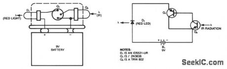
INFRARED_TRANSMITTER_1
Published:2009/7/7 8:31:00 Author:May
View full Circuit Diagram | Comments | Reading(1780)
SIMPLE_IR_DETECTOR
Published:2009/7/7 8:29:00 Author:May
This simple IR detector turns on a real LED when Q2 is exposed to invisible IR radiation found in fiber-optics systems, position sensors, and TV remote-control units. The device can be built on top of a 9-V battery and held in place with RTV. Its power dissipation is virtually zero, unless IR radiation or high ambient light is present. Normal fluorescent lighting is not a problem, but if necessary add an IR filter to the Q2 detector to exclude ambient light. Exposing the detector to a strong light or IR source gives a quick check of the battery and the red LED. (View)
View full Circuit Diagram | Comments | Reading(0)
INFRARED_TRANSMITTER
Published:2009/7/7 8:28:00 Author:May
View full Circuit Diagram | Comments | Reading(0)
DIGITAL_IR_TRANSMITTER
Published:2009/7/7 8:27:00 Author:May
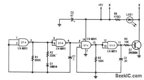
Gates U1a and U1b are configured as a low-frequency oscillator. The output waveform at pin 11 is nonsymmetrical with the positive portion of the signal, making up only 20% of the time period.Diode D1, a 1N914 general-purpose unit, together with C1, R1, and R2, determine the on time for the positive portion of the output waveform. The off, or negative portion of the output waveform, depends mainly on the values of R1 and C1. The operating frequency of that oscillator is about 11 Hz. The second oscillator consists of U1c and U1d, which outputs on almost symmetrical waveform at a frequency of about 400 Hz. The output of first oscillator U1a/U1b is fed to pin 8 of U1c to key second oscillator U1c/U1d on and off at about 11 Hz, with the on time limited to about 20% of the time period (about 15 ms).The output waveform of the second oscillator is fed to the base of Q1, which is used to drive IR diode LED1 in short bursts. Pulsing LED1 helps to save battery power, and also allows each circuit to be given its own special sound footprint.By changing any of the values of R1, R2, R3, C1, or C2, the sound footprint can be varied. As the component values are increased, the oscillator's frequency goes down, and as the values are decreased, the frequency goes up. (View)
View full Circuit Diagram | Comments | Reading(1223)
IR_TRANSMITTER
Published:2009/7/7 8:24:00 Author:May
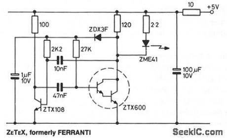
The transmitter consists of an oscillator which drives a high output IR emitting diode. The oscillator is a sure start multivibrator circuit that provides an output of 15 to 1000 mark to space ratio at a frequency of 1 kHz. This large mark to space ratio allows the IR diode to be operated at a high peak current, provided by the ZTX600 Darlington transistor, to maximize the transmitter range. A decoupling network is included in the power supply lead to isolate it from any logic circuitry using the same 5-V power supply source. The transmitter supply current is approximately 65 mA. (View)
View full Circuit Diagram | Comments | Reading(0)
IR_RECEIVER
Published:2009/7/7 8:21:00 Author:May
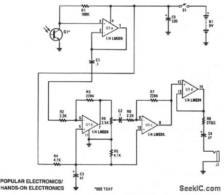
Infrared emissions detected by Q1 are fed through U1a to U1b, which amplifies the signal by a factor of 100. The amplified output of U1b is fed to U1c through R9, C2, and R6. Potentiometer R9 serves as a volume control. With R9 set to pass the maximum signal, U1c provides a gain of 100, for a total system gain of 10,000 dB. The output of U1c is connected to voltage follower circuit U1d to better match and drive headphones that can be plugged into J1. (View)
View full Circuit Diagram | Comments | Reading(1855)
| Pages:983/2234 At 209819829839849859869879889899909919929939949959969979989991000Under 20 |
Circuit Categories
power supply circuit
Amplifier Circuit
Basic Circuit
LED and Light Circuit
Sensor Circuit
Signal Processing
Electrical Equipment Circuit
Control Circuit
Remote Control Circuit
A/D-D/A Converter Circuit
Audio Circuit
Measuring and Test Circuit
Communication Circuit
Computer-Related Circuit
555 Circuit
Automotive Circuit
Repairing Circuit