
Index 310
SCHMITT_TRIGGER
Published:2009/6/30 3:46:00 Author:May
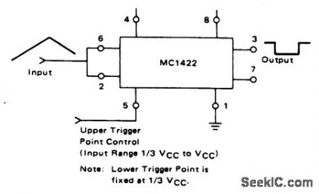
The lower trigger point is fixed at 1/3 Vcc, but the upper trigger point is adjustable by means of Pin 5 from 1/3 Vcc to slightly less than Vcc. The Schmitt triggerwill operate with input frequencies up to 50 kHz. (View)
View full Circuit Diagram | Comments | Reading(3439)
A_D_converter
Published:2009/7/24 9:46:00 Author:Jessie
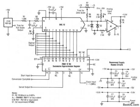
This circuit shows a DAC and comparator that is used with a 12-bit SAR to form a 10-bit A/D converter. The analog input (0 to + 10 V) is applied at R3. Both parallel and serial digital outputs are available. R7 is used to trim for zero. Full-scale is trimmed by REF-02 (Fig. 4-1C). Raytheon Linear Integrated Circuits, 1989, p. 6-28. (View)
View full Circuit Diagram | Comments | Reading(1984)
SCHMITT_TRIGGER_ZERO_CROSSING_DETECTOR_WITH_HYSTERESIS
Published:2009/6/30 3:46:00 Author:May
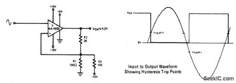
This circuit has a 100 mV hysteresis which can be used in applications where very fast transition times are required at the output even though the signal is very slow. The hysteresis loop also reduces false triggering due to noise on the input. The waveforms show the trip points developed by the hysteresis loop. (View)
View full Circuit Diagram | Comments | Reading(1117)
Offset_binary_D_A_converter_operation
Published:2009/7/24 9:42:00 Author:Jessie
This circuit shows a DAC/op-amp combination that is used to provide offset-binary operation. Raytheon Linear Integrated Circuits, 1989, p. 6-14. (View)
View full Circuit Diagram | Comments | Reading(1)
SCHMITT_TRIGGER_WITH_PROGRAMMABLE_HYSTERESIS
Published:2009/6/30 3:44:00 Author:May
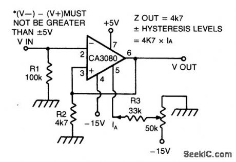
CA 3088 is used as a versatile Schmitt trigger. The size of the hysteresis levels is determined by IA that flows out of the amplifier's output and through R2. Increasing IA increases hysteresis and vice versa. The positive and negative hysteresis levels are symmetrical about 0 V. (View)
View full Circuit Diagram | Comments | Reading(885)
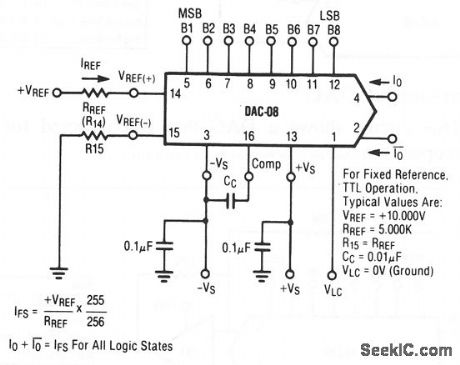
Basic_bipolar_output_DAC
Published:2009/7/24 9:41:00 Author:Jessie
This circuit shows a DAC that is connected for bipolar-output D/A-converter operation. Raytheon Linear Integrated Circuits, 1989, p. 6-14. (View)
View full Circuit Diagram | Comments | Reading(0)
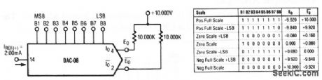
Basic_unipolar_negative_reference_DAC
Published:2009/7/24 9:41:00 Author:Jessie
This circuit shows a DAC that is connected for unipolar negative-reference D/A-converter operation. Raytheon Linear Integrated Circuits, 1989, p. 6-13. (View)
View full Circuit Diagram | Comments | Reading(613)
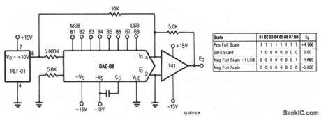
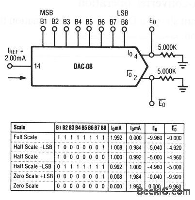
Basic_positive_reference_DAC
Published:2009/7/24 9:40:00 Author:Jessie
This circuit shows a DAC that is connected for D/A-converter operation. Raytheon Linear Integrated Circuits, 1989, p. 6-12. (View)
View full Circuit Diagram | Comments | Reading(871)
Three_input_AND_gate
Published:2009/7/24 9:39:00 Author:Jessie
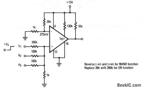
This circuit uses an LP165/365 comparator as a 3-input AND gate. The circuit can be converted to NAND or OR, as shown. Raytheon Linear Integrated Circuits, 1989, p. 5-43. (View)
View full Circuit Diagram | Comments | Reading(884)
TTL_to_MOS_logic_converter
Published:2009/7/24 9:37:00 Author:Jessie
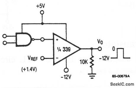
This circuit uses a 339 comparator to convert from TTL to MOS logic. Raytheon Linear Integrated Circuits, 1989, p. 5-31. (View)
View full Circuit Diagram | Comments | Reading(1742)
SCHMITT_TRIGGER_WITHOUT_HYSTERESIS
Published:2009/6/30 3:43:00 Author:May
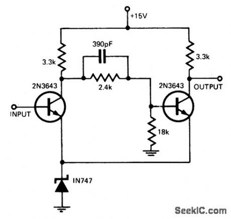
By replacing the common-emitter resistor in a conventional Schmitt by a zener diode, the hysteresis normally associated with these circuits is eliminated. (View)
View full Circuit Diagram | Comments | Reading(952)
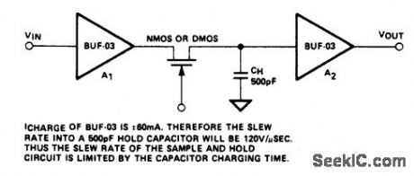
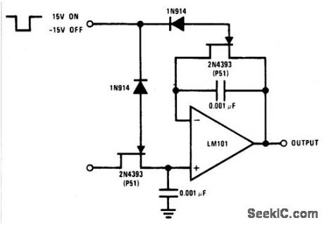
HIGH_SPEED_SAMPLE_AND_HOLD_2
Published:2009/6/30 3:41:00 Author:May
View full Circuit Diagram | Comments | Reading(482)
HIGH_ACCURACY_SAMPLE_AND_HOLD
Published:2009/6/30 3:39:00 Author:May

View full Circuit Diagram | Comments | Reading(556)
SAMPLE_AND_HOLD
Published:2009/6/30 3:39:00 Author:May
View full Circuit Diagram | Comments | Reading(1601)
×1000_SAMPLE_AND_HOLD
Published:2009/6/30 3:37:00 Author:May
(View)
View full Circuit Diagram | Comments | Reading(445)
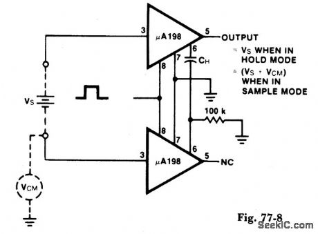
DIFFERENTIAL_HOLD
Published:2009/6/30 3:36:00 Author:May
View full Circuit Diagram | Comments | Reading(626)
EXCESS_THREE_GRAY_CODE_TO_BCD
Published:2009/6/30 3:36:00 Author:May
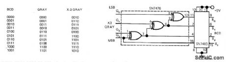
Develped for use with shaft encoder providing excess-three Gray-code output Requires only two TTL ICs, connected as shown. To convert regular Gray code to BCD, omit SN7483 4-bit adder.Tabulation shows how circuit accomplishes conversion for both types of Gray codes.—D. M. Risch, Two ICs Convert Excess-Three Gray Code to BCD, EDN Magazine, Nov. 1, 1972, p 44. (View)
View full Circuit Diagram | Comments | Reading(1845)
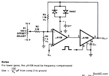
SAMPLE_AND_HOLD_WITH_OFFSET_ADJUSTMENT
Published:2009/6/30 3:35:00 Author:May
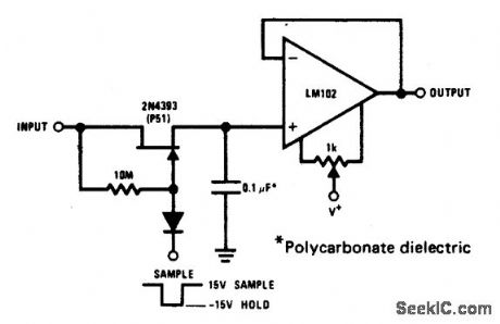
The 2N4393 JFET was selected because of its low IGss (<100 pA), very low ID(off) (< 100 pA) and low pinchoff voltage. Leakages of this level put the burden of circuit performance on clean, solder-resin free, low leakage circuit layout. (View)
View full Circuit Diagram | Comments | Reading(1454)
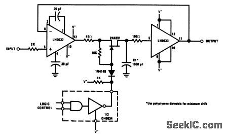
HIGH_SPEED_SAMPLE_AND_HOLD
Published:2009/6/30 3:31:00 Author:May
View full Circuit Diagram | Comments | Reading(1131)
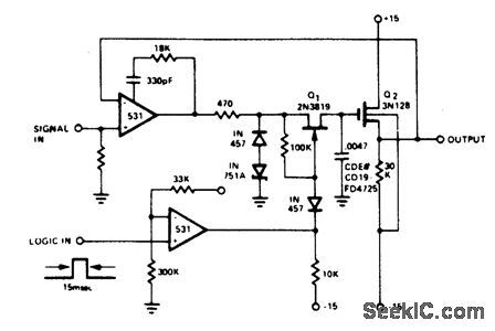
JFET_SAMPLE_AND_HOLD
Published:2009/6/30 3:24:00 Author:May
The logic voltage is applied simultaneously to the sample and hold JFETs. By matching input impedance and feedback resistance and capacitance, errors due to rds(on) of the JFETs are minimized. (View)
View full Circuit Diagram | Comments | Reading(942)
| Pages:310/471 At 20301302303304305306307308309310311312313314315316317318319320Under 20 |
Circuit Categories
power supply circuit
Amplifier Circuit
Basic Circuit
LED and Light Circuit
Sensor Circuit
Signal Processing
Electrical Equipment Circuit
Control Circuit
Remote Control Circuit
A/D-D/A Converter Circuit
Audio Circuit
Measuring and Test Circuit
Communication Circuit
Computer-Related Circuit
555 Circuit
Automotive Circuit
Repairing Circuit