
Index 301
VARIABLE_PULSE_WIDTH
Published:2009/7/1 5:36:00 Author:May
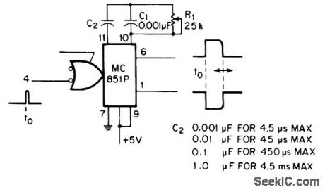
R1 and C2 together provide wide range of pulse widths from Motorola MC851P mono. Rise and fall times of complementary output pulses are better than 100 μs. With only four switched capacitors in combination whh R1, pulse widths can be varied between maximum of 4.5 ms and minimum well under 4.5 μs.-C. W. Stoops, Wide-Range Variable Pulse-Width Monostable, EEE Maga-zine,.Dec. 1970, p 56. (View)
View full Circuit Diagram | Comments | Reading(737)
FREQUENCY_DOUBLING_TACHOMETER
Published:2009/7/1 5:35:00 Author:May
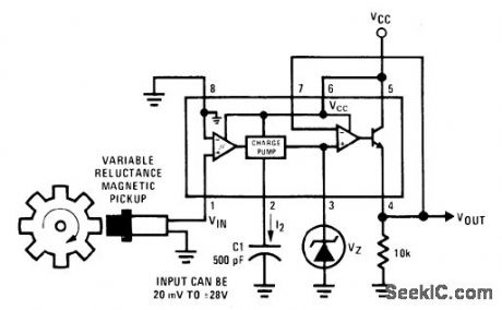
Connection shown for National LM2907 IC provides output pulse each time sine-wave input from magnetic pickup crosses zero, for use in digital control system. Width of each pulse is determined by size of C1 and supply voltage used.Circuit serves for doubling frequency presented to microprocessor control system.- Linear Applications, Vol. 2, National Semiconductor, Santa Clara, CA, 1976, AN-162, p12-13. (View)
View full Circuit Diagram | Comments | Reading(3262)
LOW_COST“HEADS_OR_TAILS”
Published:2009/7/1 5:33:00 Author:May
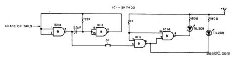
Circuit NotesS1 must be a push-to-make, release-to-break, switch. (View)
View full Circuit Diagram | Comments | Reading(456)
OUTBAND_DESCRAMBLER
Published:2009/7/1 5:32:00 Author:May
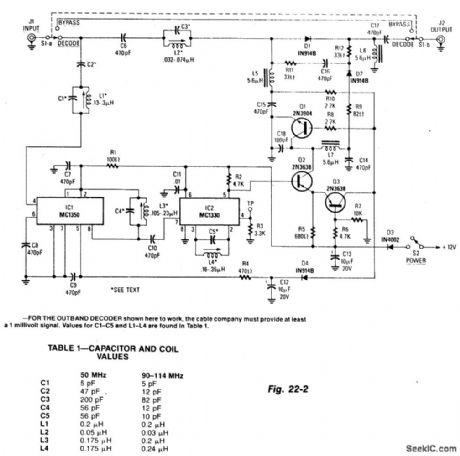
This circuit consists of an amplifier for the synch channel and a video detector which controls an attenuator so that the gain of the systems is increased during synch intervals. Kit available from North Country Radio, P.O. Box 53, Wykagyl Station, New York 10804. (View)
View full Circuit Diagram | Comments | Reading(1386)
POT_SHOT
Published:2009/7/1 5:31:00 Author:May
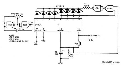
Circuit Notes
This is a circuit for a game of the shooting gallery variety. IC2a and b form an astable multivibrator clocking IC1 which causes LEDs 1-8 to flash in turn LED 5 is the target LED and the object of the game is to depress PBI just as LED 5 comes on. If this is done, the whole display is blanked for a few seconds signifying a hit. Otherwise, the LED which was lit remains lit. When the push button is released, C2 dis-charges through R2 taking 8 pin 13 low again and the LEDs will start to flash again. (View)
View full Circuit Diagram | Comments | Reading(838)
PWM_MONO
Published:2009/7/1 5:30:00 Author:May
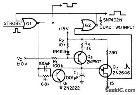
Circuit provides pulse-width modulation with high duty cycles and comple-mentary output, Strobe input to gate G1 drives output of gate to binary 0, turning Q1 off and letting voltageacross C1 build up until UJT Q3 fires, discharging C1. Output of UJT drives output of G2 to binary 0. Article gives timing diagrams.-G. Lewis. Simple One Shot Has Complementary Outputs, EEEMagazine. Oct. 1970. p 78-79. (View)
View full Circuit Diagram | Comments | Reading(643)
FREQUENCY_INDICATOR_
Published:2009/7/1 5:29:00 Author:May
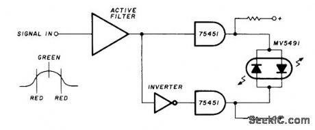
|Circuit furnishes green indication at resonance and red for either side of resonance. Uses Monsanto MV5491 dual redlgreen LED, with 220 ohms in upper lead to +5 V supply and 100 ohms in lower +5 V lead because red and green LEDs in parallel back-to-back have different voltage requirements. Useful for SSTV, RTTY, or subaudio-tone indication for control purposes on FM. Circuit requires two driver ICs and one section of hex inverter IC, with any suitable active filter used to form level detector for signals at desired frequency.-K.Powell, Novel Indicator Circuit, Ham Radio, April 1977, p 60-63. (View)
View full Circuit Diagram | Comments | Reading(735)
FUZZ__BOX__1
Published:2009/7/1 5:26:00 Author:May
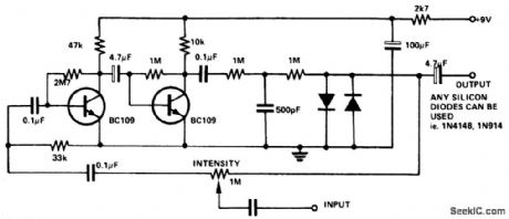
Circuit NotesThe input signal is amplified by the transistors. The distorted output is then clipped by the two diodes and the high frequency noise is filtered from the circuit via the 500 pF capacitor. The 1 M pot adjusts the intensity of the fuzz frog maximum to no fuzz (normal playing). (View)
View full Circuit Diagram | Comments | Reading(881)
GATE_DIPPER
Published:2009/7/1 5:24:00 Author:May

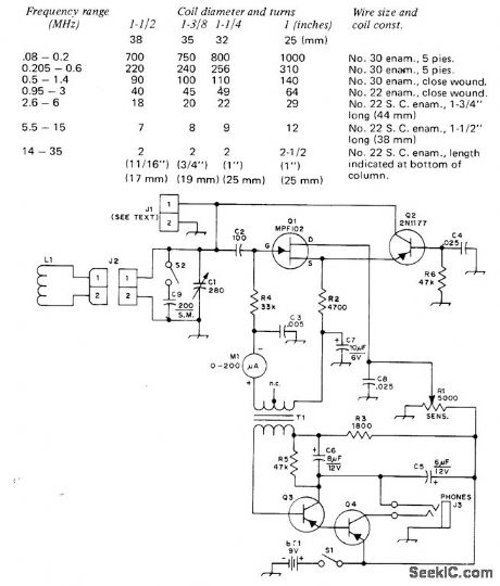
Used to determine resonant frequency of tuned circuit, provide signal for re-ceiver alignment, and make antenna measure-ments. Table gives winding data for plug-in coils L1. Parts values are not critical. T2 is tran-sistor interstage audio transformer with 10,000-ohm primary and 2,000-ohm secondary in meter circuit. JFET a1 is used in common-drain circuit followed by PNP bipolar transistor, with gate junction of JFET acting as rectifier. Dip meter M1 measures gate current, When tuned circuit of dipper is Ioaded by coupling it to extemal cir-cuit, power is absorbed and meter reads dip occurring when L1-C1 is tuned to resonance with external circuit. R1 is regeneration control.Audio amplifer 03-04 using 2N4125 or HEP52, optional, helps in Iistening to signals picked up by tuned circuit or enhances display on CROCan be used as field-strength meter if antenna is plugged into J1.-B. Clark, A Hybrid Gate-Dip Osdllator, QST, June 1974, p 33-37. (View)
View full Circuit Diagram | Comments | Reading(905)
POSITIVE_OUTPUT_MONO
Published:2009/7/1 5:23:00 Author:May
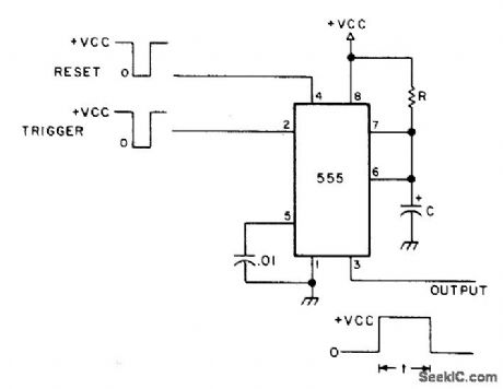
Timer is triggered by negative-going pulse to give positive output pulse whose width t in seconds is 1.1RC. VCC is 4.5-16 V at 3-10 mA.-H. M. Berlin, IC Timer Review, 73 Magazine, Jan. 1978, p 40-45. (View)
View full Circuit Diagram | Comments | Reading(705)
6_DIGIT_FOUR_FUNCTION
Published:2009/7/1 5:22:00 Author:May
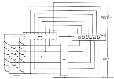
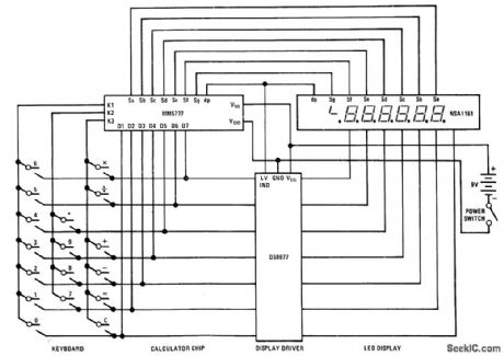
National MM5777 calculator chip requires only keyboard, NSA1161 LED display, DS8977 digit driver, and 9-V battery to provide add, subtract, multiply, and divide functions. Calculator chip includes keyboard encoding and key debouncing circuits, along with all clock and timing generators. LED segments can be driven directly, without multiplexing. Seventh digit position is used for negative sign of 6-digit number and as error indicator.Leading and trailing zero suppressionis included.-, MOS/LSI Databook, National Semiconductor,Santa Clara,GA,1977,p 8-84-8-89. (View)
View full Circuit Diagram | Comments | Reading(1371)
BCD_DECODER
Published:2009/7/1 5:21:00 Author:May

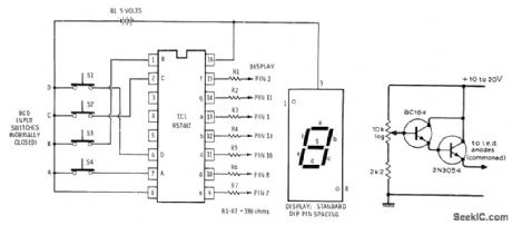
Radio Shack RS7447 BCD to 7-segment decoder converts settings of four BCD input switches to corresponding 0-9 digit on 7-segment commonanode LED display. Display is Radio Shack 276-053. Battery can be four AA cells in series,with 1N914 diodeinserted in positive lead to reduce voltage to 5 v.-F.m.Mims, Integrated Cirouit Proieets, Vol 2, Radio Shack,Fort Worth,TX,1977,2nd Ed.p 27-40. (View)
View full Circuit Diagram | Comments | Reading(3438)
001_Hz_to_7_MHz
Published:2009/7/1 5:20:00 Author:May
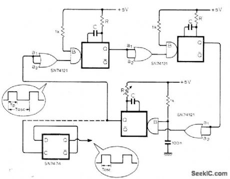
Generates square waves suitable for clock signals in sequential digital circuits, with values of RC pairs determining period in rangefrom about 150 ns to 120 s. To obtain equal mark-space ratio, set oscillator to half the required period and add bistable SN7474 divider as shown by dashed line,-P. J. Best, Monostable Ring Oscillator. Wireless World. March 1976. p 89. (View)
View full Circuit Diagram | Comments | Reading(688)
SINE_WAVE_DESCRAMBLER
Published:2009/7/1 5:16:00 Author:May
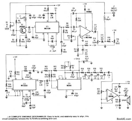
This decoder features a sine wave recovery channel and uses a PIN diode attenuator driven by the she wave recovery system to cancel out the she wave sync suppression signal. Kit available from North Country Radio, P.O. Box 53, Wykagyl Station, New York 10804. (View)
View full Circuit Diagram | Comments | Reading(1962)
VERSATILE_MONO
Published:2009/7/1 5:15:00 Author:May
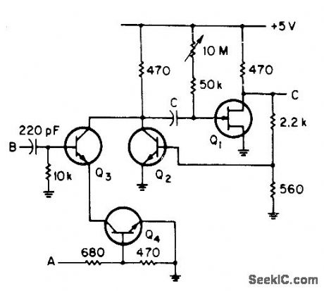
Uses standard digital IC voltage levels as inputs, and can be enabled or inhibited at any time without causing output pulse. Input gate Q3-Q4 is enabled with logic 1 at point A and inhibited with logic O.Logic 1 at B starts timing cycle. Q1 is 2N3819 JFET, and all other transistors are 2N3704.-R. Tenny, Versatile One-Shop, EEE Magazine, Sept. 1970, p 89 (View)
View full Circuit Diagram | Comments | Reading(637)
AM_DEMODULATOR
Published:2009/7/1 5:12:00 Author:May
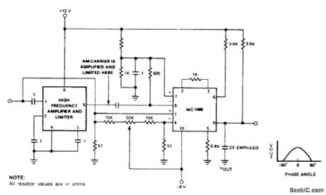
Amplifying and limiting of the AM carrier is accomplished by the if gain block providing 55 dB of gain or higher with a limiting of 40 μV. The limited carrier is then applied to the detector at the carrier ports to provide the desired switching function. The signal is then demodulated by the synchronous AM demodulator (1496) where the carrier frequency is attentuated due to the balanced nature of the device. Care must be taken not to overdrive the signal input so that distortion does not appear in the recorded audio.Maximum conversion gain is reached when the carrier signals are in phase as indicated by the phase-gain relationship. Output ftltering is also necessary to remove high frequency sum components of the carrier from the audio signal. (View)
View full Circuit Diagram | Comments | Reading(3138)
STEREO_DEMODULATOR
Published:2009/7/1 5:09:00 Author:May
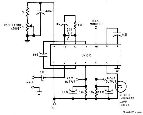
This circuit uses a single IC LM1310 to provide left and right outputs from a composite MPX stereo signal. Oscillator adjust R1 is set for 76 kHz (19 kHz at pin 10). C1 should be a silver mica or NPO ceramic capacitor. (View)
View full Circuit Diagram | Comments | Reading(1543)
NARROW_BAND_FM_DEMODULATOR_WITH_CARRIER_DETECT
Published:2009/7/1 5:07:00 Author:May
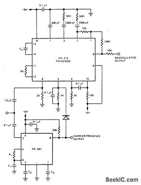
For FM demodulation applications where the bandwidth is less than 10% of the carrier frequency, an XR-567 can be used to detect the presence of the carrier signal. The output of the XR-567 is used to turn off the FM demodulator when no carrier is present, thus acting as a squelch. In the circuit shown, an XR-215 FM demodulator is used because of its wide dynamic range, high signal/noise ratio and low distortion.The XR-567 will detect the presence of a carrier at frequencies up to 500 kHz. (View)
View full Circuit Diagram | Comments | Reading(1270)
TRIGGERED_BISTABLE
Published:2009/7/1 5:06:00 Author:May
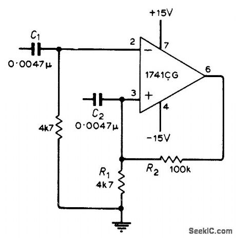
Positive feedback applied to opamp through R2 and R1 causes amplifier output to remain at either its positive or negative saturation limit. Triggering pulses for changing state of output may be applied to either input terminal, through C1 or C2; pulse polarity required to produce transition depends on state of circuit, which should be verified ex-perimentally.-G. B. Clayton, Experiments with Operational Amplifiers. Wireless World, May 1973. p 241-242. (View)
View full Circuit Diagram | Comments | Reading(709)
15_s_ASTABLE
Published:2009/7/1 5:01:00 Author:May
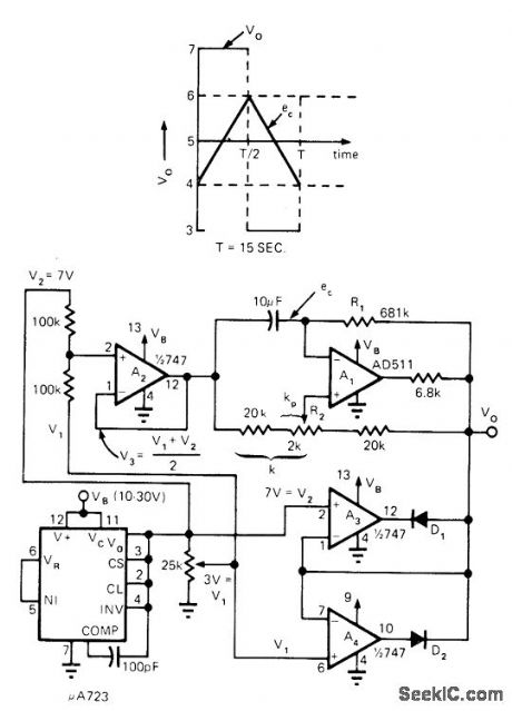
Precision opamp/diode clamp circuit simulating zener reduces cost of astable multivibrator having long time constant and good temperature stability. Circuit operates from single-ended supply, with μA723 providing 7-V referencefor clamp amplifiers A3 and A4. A2 provides oscillator with reference voltage V3 halfway between V1 and V2. R2 allows frequency of oscillator to be adjusted about ±6%. Article gives design equations.-L. Drake. Long Time-Constant Oscillator Uses Precision Clamps, EDN Magazine, Dec. 20, 1974, p 51-52. (View)
View full Circuit Diagram | Comments | Reading(741)
| Pages:301/471 At 20301302303304305306307308309310311312313314315316317318319320Under 20 |
Circuit Categories
power supply circuit
Amplifier Circuit
Basic Circuit
LED and Light Circuit
Sensor Circuit
Signal Processing
Electrical Equipment Circuit
Control Circuit
Remote Control Circuit
A/D-D/A Converter Circuit
Audio Circuit
Measuring and Test Circuit
Communication Circuit
Computer-Related Circuit
555 Circuit
Automotive Circuit
Repairing Circuit