
Index 315
Universal_state_variable_filter
Published:2009/7/24 14:01:00 Author:Jessie
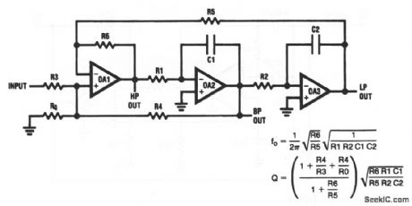
This circuit uses three op amps to form a universal state-variable filter. Compare this circuit and equations to that of Fig. 7-6. National Semiconductor, Linear Applications Handbook, 1991, p. 903. (View)
View full Circuit Diagram | Comments | Reading(2388)
1_kHz_bandpass_filter_with_high_Q
Published:2009/7/24 14:00:00 Author:Jessie
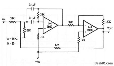
This circuit uses two sections of a 3900 op amp to form a high-Q (Q=25) bandpass filter. Raytheon Linear Integrated Circuts, 1989, p. 4.274. (View)
View full Circuit Diagram | Comments | Reading(1659)
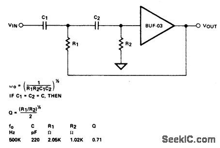
1_kHz_bandpass_filter
Published:2009/7/24 13:59:00 Author:Jessie
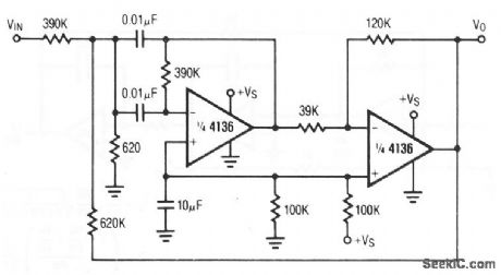
This circuit uses two sections of a 4136 op amp to form a bandpass filter. Raytheon Linear Integrated Circuts, 1989, p. 4-175. (View)
View full Circuit Diagram | Comments | Reading(862)
Dc_accurate_low_pass_bandbass_filter
Published:2009/7/24 13:58:00 Author:Jessie
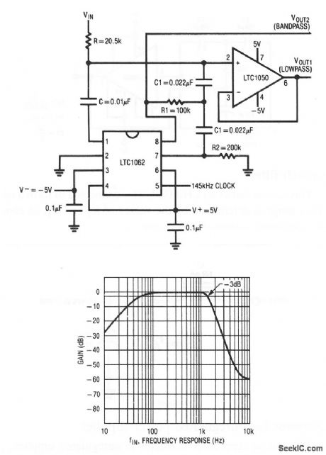
This circuit uses an LTC1050 and LTC1062 to form a filter that extracts ac information from a dc +ac signal. Figure 7-48B shows the bandpass-filter output characteristics. Linear Technology, Linear Appications Handbook, 1990, p. DN9-2. (View)
View full Circuit Diagram | Comments | Reading(572)
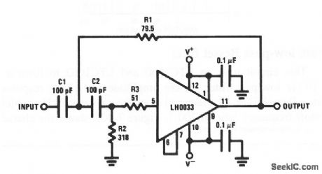
45_MHz_notch_filter
Published:2009/7/24 13:54:00 Author:Jessie
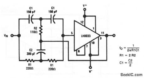
This circuit shows an LH0033 buffer connected to form a notch filter. The frequency range is determined by the values of R1 and C1, as shown by the equation. National Semiconductor, Linear Applications Handbook, 1991, p. 161. (View)
View full Circuit Diagram | Comments | Reading(622)
Fed_forward_low_pass_filter
Published:2009/7/24 13:53:00 Author:Jessie
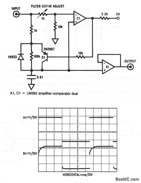
This circuit allows a signal to be rapidly acquired to final value, but it provides a long filtering constant. Such a characteristic is useful in multiplexed data-acquisition systems, and has been used in electronic infant-weighing scales, where fast, stable readings of weight are needed (in spite of motion on the scale platform). The point at which the filter switches from a short to a long time constant is set by the 1-kΩ pot. Normally, this is adjusted so that switching-occurs at 90% to 98% of final value. However, the waveforms shown in Fig. 7-45B were obtained at a 70% trip point to show circuit operation. National Semiconductor, Linear Applications Handbook, 1991, p. 835. (View)
View full Circuit Diagram | Comments | Reading(613)
Ultrasonic_filter
Published:2009/7/24 13:51:00 Author:Jessie
This circuit shows both sections of an LM833 that is connected as a filter to reject undesired ultrasonic signals. The filter characteristic is 4th-order Bessel with the -3-dB frequency at about 40 kHz. Resistors and capacitors should be 1%-tolerance components. This circuit can be cascaded with that of Fig. 7-43 (with the low-pass preceding the high-pass) to produce a response such as shown in Fig. 7-44B. National Semiconductor, Linear Applications Handbook, 1991, p. 944,945. (View)
View full Circuit Diagram | Comments | Reading(2920)
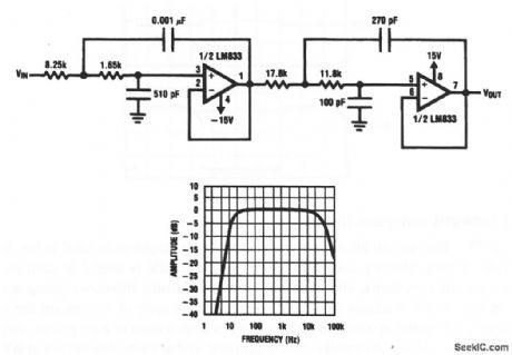
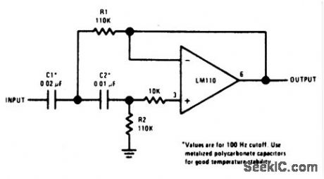
Infrasonic_filter
Published:2009/7/24 13:51:00 Author:Jessie
This circuit shows an LM833 connected as a filter for rejecting undesired infrasonic signals. The filter characteristic is 3rd-order Butterworth with the -3-dB frequency at 15 Hz. Resistors and capacitors should be 1%-tolerance components (although 5%-tolerance components can be substituted in less critical applications). National Semiconductor, Linear Applications Handbook, 1991, p. 944. (View)
View full Circuit Diagram | Comments | Reading(946)
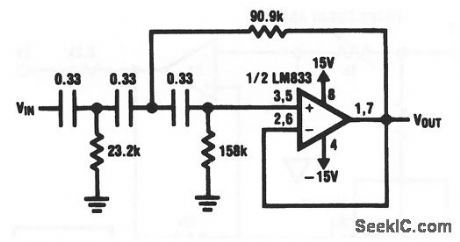
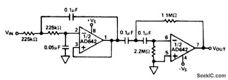
Wideband_two_pole_high_pass_filter
Published:2009/7/24 13:50:00 Author:Jessie
This circuit shows an LH0033 buffer connected to form a basic two-pole high-pass filter with a 10-Hz cutoff frequency. A low-pass filter with the same frequency can be obtained by interchanging R1, R2, C1, and C2. National Semiconductor, Linear Applications Handbook, 1991, p. 542. (View)
View full Circuit Diagram | Comments | Reading(1793)
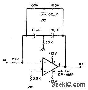
EQUALIZER
Published:2009/6/30 2:14:00 Author:May
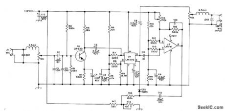
Designed for use between input jack and microphone of amateur transmitter, to keep bandpass response between limits of about 200 and 3100Hz. Circuit also provides measure of volume compression, improving transmitter efficiency. Construction and ad justment details stress importance of eliminating ground loops and RF feedback. Un is voltage-controlled amplifier in feedback loop, with 741 opamp U2 as compression detector. U2 is biased so output is almost at ground, and no feedback voltage is applied until input to U2 exceeds 0.9 V. U: thus operates in linear mode at maximum gain until output voltage exceeds 0.9 V, when voltage is applied to UI and gain of IC is reduced.-R. Tauber, The Equalizer, QST, March 1977, p 18-20. (View)
View full Circuit Diagram | Comments | Reading(2574)
CLAMPING_WITH_OPAMPS
Published:2009/6/30 2:12:00 Author:May
Circuit is used after stage of AC amplification to damp minimum level of signal voltage to 0 V for signals having amplitudes between 10mV and 10V.With 250-μF electrolytic for C, sinusoidal waveforms between 3 and 10,000 Hz are clamped with little distortion. Overall gain is unity,-C.B. Mussell, D.C.Level Clamp, Wireless World, Feb. 1975, p 93. (View)
View full Circuit Diagram | Comments | Reading(921)
AF_COMPRESSOR
Published:2009/6/30 2:12:00 Author:May
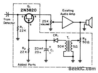
Developed for use in communication receiver where signals vary so greatly that even modern AVC systems cannot level all signals. Circuit is AVC that sets miaxmum audio level which will not be exceeded.Uses one FET as series attenuator controlled by DC voltage derived from audio output. R3 permits adjustment of compression leveL-C.E.Richmond, A Receiver Audio Compressor, CQ June1970,p 35 and 86. (View)
View full Circuit Diagram | Comments | Reading(1385)
28_V_HIGH_EFFICIEIVCY
Published:2009/6/30 2:09:00 Author:May
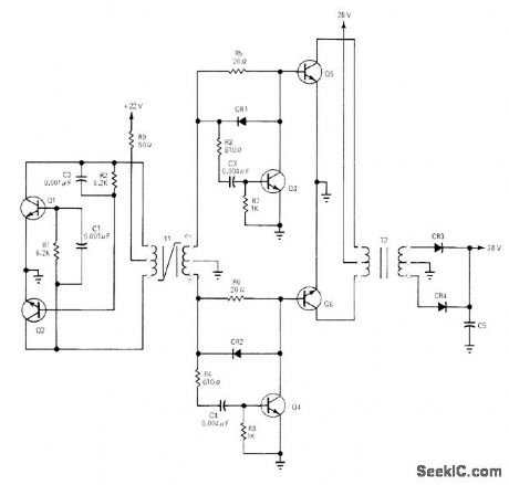
Uses driven-type converter in which signal source is simple two-transistor oscillator Q1-Q2. Turn-on delay technique eliminates overlap current otherwise flowing in 2N1016 push-pull power transistors Q5 and Q6 when one is still on in storage state while other is driven on. Efficiency can approach 90%. Q3 and Q4 prevent off transistor from conducting until opposite device has turned off. Values for T2, CR3, and CR4 in output circuit are chosen to give desired DC output voltage.—R. F. Downs, Minimize Overlap to Maximize Efficiency in Saturated Push-Pull Circuits, EDN|EEE Magazine, Feb. 1, 1972, p 48-50. (View)
View full Circuit Diagram | Comments | Reading(526)
160_Hz_BANDPASS_FILTER_
Published:2009/6/30 2:07:00 Author:May
View full Circuit Diagram | Comments | Reading(643)
SECOND_ORDER___HIGH_PASS_ACTIVE_FILTER___
Published:2009/6/30 2:07:00 Author:May
View full Circuit Diagram | Comments | Reading(797)
BATTERY_LIFE_EXTENDER
Published:2009/6/30 2:05:00 Author:May
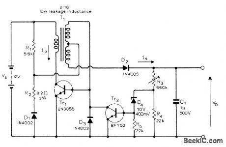
Conserves battery life by charging capacitor from 0 V at efficiencies over 80% and by allowing battery to be used to lower endpoint voltage, Will generate voltages above or below battery voltages. When used in capacitor-discharge ignition system, power conversion efficiency is so high that heatsink is unnecessary and only one power transistor is needed. Givesfull output voltage even when car battery voltage is less than half nominal value, as during cold starting. Article describes operation of circuit in detail. Tr1 may require series RC protection between collector and emitter.—R. M. Carter, Variable Voltage-Ratio Transistor Converter, Wireless World, Nov. 1975, p 519. (View)
View full Circuit Diagram | Comments | Reading(2944)
12V_TO__11_V_WITH_CMOS_IC
Published:2009/6/30 2:04:00 Author:May
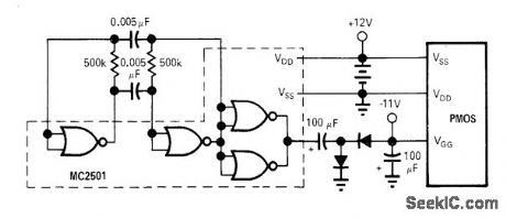
Bipolar inverter and rectifier together provide -11 V from 12-V auto battery for operating high-threshold MOS logic of portable or automotive equipment.Diode types are not critical. Inverter draws only about 1 mA from 12.V battery on standby and supplies 2 mA from -11V terminal.—B. Fette, Inexpensive Inverters Generate VGG for Portable MOS Applications, EDN|EEE Magazine, Dec. 15, 1971,p 51. (View)
View full Circuit Diagram | Comments | Reading(549)
HIGH_PASS_FILTER(HIGH_FREQUENCY)
Published:2009/6/30 2:04:00 Author:May
View full Circuit Diagram | Comments | Reading(593)
HIGH_PASS_ACTIVE_FILTER
Published:2009/6/30 2:03:00 Author:May
View full Circuit Diagram | Comments | Reading(0)
01_Hz_TO_10_Hz_BANDPASS_FILTER
Published:2009/6/30 2:03:00 Author:May
View full Circuit Diagram | Comments | Reading(954)
| Pages:315/471 At 20301302303304305306307308309310311312313314315316317318319320Under 20 |
Circuit Categories
power supply circuit
Amplifier Circuit
Basic Circuit
LED and Light Circuit
Sensor Circuit
Signal Processing
Electrical Equipment Circuit
Control Circuit
Remote Control Circuit
A/D-D/A Converter Circuit
Audio Circuit
Measuring and Test Circuit
Communication Circuit
Computer-Related Circuit
555 Circuit
Automotive Circuit
Repairing Circuit